Kürzlich haben wir festgestellt, dass Kriminelle vorgaben, AiPCBA zu sein, um zu betrügen oder zu versuchen, Fälschungen zu verkaufen
ausgefallene Komponenten zu günstigen Preisen.
AiPCBA hat ein
Komponentenprüflabor
im Jahr 2021 mit dem Ziel, qualitätsgesicherte Komponenten bereitzustellen.
Wir empfehlen unseren Kunden dringend, sich für zuverlässige Komponentenlieferanten zu entscheiden.
Bitte beachten Sie, dass die einzigen offiziellen Website- und E-Mail-Suffixe sind
aipcba.com
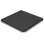
NXP® Semiconductors designed the LPC2420/2460 microcontroller around a 16-bit/32-bit ARM7TDMI-S CPU core with real-time debug interfaces that include both JTAG and embedded trace. The LPC2420/2460 is flashless. The LPC2420/2460 can execute both 32-bit ARM and 16-bit Thumb instructions. Support for the two instruction sets means engineers can choose to optimize their application for either performance or code size at the sub-routine level. When the core executes instructions in Thumb state it can reduce code size by more than 30 % with only a small loss in performance while executing instructions in ARM state maximizes core performance.
The LPC2420/2460 microcontroller is ideal for multi-purpose communication applications. It incorporates a 10/100 Ethernet Media Access Controller (MAC) (LPC2460 only), a USB full-speed device/host/OTG controller with 4 kB of endpoint RAM, four UARTs, two Controller Area Network (CAN) channels (LPC2460 only), an SPI interface, two Synchronous Serial Ports (SSP), three I²C interfaces, and an I²S interface. Supporting this collection of serial communications interfaces are the following feature components; an on-chip 4 MHz internal precision oscillator, 82/98 kB of total RAM consisting of 64 kB of local SRAM, 16 kB SRAM for Ethernet (LPC2460 only), 16 kB SRAM for general purpose DMA, 2 kB of battery powered SRAM, and an External Memory Controller (EMC). These features make this device optimally suited for communication gateways and protocol converters. Complementing the many serial communication controllers, versatile clocking capabilities, and memory features are various 32-bit timers, an improved 10-bit ADC, 10-bit DAC, two PWM units, four external interrupt pins, and up to 160 fast GPIO lines. The LPC2420/2460 connects 64 of the GPIO pins to the hardware based Vector Interrupt Controller (VIC) that means these external inputs can generate edge-triggered interrupts. All of these features make the LPC2420/2460 particularly suitable for industrial control and medical systems.
MoreLess
## Features
* ARM7TDMI-S processor, running at up to 72 MHz.
* 82/98 kB on-chip SRAM includes:
* 64 kB of SRAM on the ARM local bus for high performance CPU access.
* 16 kB SRAM for Ethernet interface. Can also be used as general purpose SRAM. (LPC2460 only)
* 16 kB SRAM for general purpose DMA use also accessible by the USB.
* 2 kB SRAM data storage powered from the Real-Time Clock (RTC) power domain.
* Dual Advanced High-performance Bus (AHB) system allows simultaneous Ethernet DMA, and USB DMA with no contention (LPC2460 only).
* EMC provides support for asynchronous static memory devices such as RAM, ROM and flash, as well as dynamic memories such as single data rate SDRAM.
* Advanced Vectored Interrupt Controller (VIC), supporting up to 32 vectored interrupts.
* General Purpose DMA controller (GPDMA) on AHB that can be used with the SSP, I²S, and SD/MMC interface as well as for memory-to-memory transfers.
* Serial Interfaces:
* Ethernet MAC with MII/RMII interface and associated DMA controller (LPC2460 only). These functions reside on an independent AHB.
* USB 2.0 full-speed dual port device/host/OTG controller with on-chip PHY and associated DMA controller.
* Four UARTs with fractional baud rate generation, one with modem control I/O, one with IrDA support, all with FIFO.
* CAN controller with two channels (LPC2460 only).
* SPI controller.
* Two SSP controllers, with FIFO and multi-protocol capabilities. One is an alternate for the SPI port, sharing its interrupt. SSPs can be used with the GPDMA controller.
* Three I²C-bus interfaces (one with open-drain and two with standard port pins).
* I²S (Inter-IC Sound) interface for digital audio input or output. It can be used with the GPDMA.
* Other peripherals:
* SD/MMC memory card interface.
* 160 General purpose I/O pins with configurable pull-up/down resistors.
* 10-bit ADC with input multiplexing among 8 pins.
* 10-bit DAC.
* Four general purpose timers/counters with 8 capture inputs and 10 compare outputs. Each timer block has an external count input.
* Two PWM/timer blocks with support for three-phase motor control. Each PWM has an external count inputs.
* RTC with separate power domain. Clock source can be the RTC oscillator or the APB clock.
* 2 kB SRAM powered from the RTC power pin, allowing data to be stored when the rest of the chip is powered off.
* WatchDog Timer (WDT). The WDT can be clocked from the internal RC oscillator, the RTC oscillator, or the APB clock.
* Standard ARM test/debug interface for compatibility with existing tools.
* Four reduced power modes: idle, sleep, power-down, and deep power-down.
* Four external interrupt inputs configurable as edge/level sensitive. All pins on port 0 and port 2 can be used as edge sensitive interrupt sources.
* Processor wake-up from Power-down mode via any interrupt able to operate during Power-down mode (includes external interrupts, RTC interrupt, USB activity, port 0/2 pin interrupt, Ethernet wake-up interrupt (LPC2460 only), CAN bus activity (LPC2460 only)).
* Two independent power domains allow fine tuning of power consumption based on needed features.
* Each peripheral has its own clock divider for further power saving. These dividers help reduce active power by 20 % to 30 %.
* Brownout detect with separate thresholds for interrupt and forced reset.
* On-chip power-on reset.
* On-chip crystal oscillator with an operating range of 1 MHz to 25 MHz.
* 4 MHz internal RC oscillator trimmed to 1 % accuracy that can optionally be used as the system clock. When used as the CPU clock, does not allow CAN and USB to run.
* On-chip PLL allows CPU operation up to the maximum CPU rate without the need for a high frequency crystal. May be run from the main oscillator, the internal RC oscillator, or the RTC oscillator.
* Boundary scan for simplified board testing.
* Versatile pin function selections allow more possibilities for using on-chip peripheral functions.
Die hier aufgeführten Geschäftsbedingungen dienen nur als Referenz, die tatsächlichen AGB unterliegen dem Angebot des Verkäufers. - Bitte bestätigen Sie die Spezifikationen der Produkte bei der Bestellung. - MOQ bedeutet die Mindestbestellmenge, die erforderlich ist, um jedes Teil zu kaufen. - Wenn Sie spezielle Bestellanweisungen haben, vermerken Sie diese bitte auf der Bestellseite. - Die Pre-Shipment Inspection (PSI) wird angewendet. - Sie können uns jederzeit eine E-Mail senden, um den Bestellstatus zu überprüfen. - Bestellungen können nach Versand der Pakete nicht mehr storniert werden.
- TT im Voraus (Banküberweisung), PayPal kann ausgewählt werden. - Nur Barüberweisung. (Überweisungen mit Schecks und Wechseln werden nicht akzeptiert.) - Der Kunde ist für die Zahlung aller möglichen Gebühren verantwortlich, einschließlich Umsatzsteuer, Mehrwertsteuer und Zollgebühren usw. - Wenn Sie die detaillierte Rechnung oder Steuernummer benötigen, senden Sie uns bitte eine E-Mail.
- FedEx, DHL und UPS können ausgewählt werden. - Sie können auswählen, ob die Versandkosten von Ihrem Versandkonto oder von unserer Seite berechnet werden sollen. - Bitte bestätigen Sie dies im Voraus mit dem Logistikunternehmen, wenn Sie sich in einem abgelegenen Gebiet befinden.
(Es können zusätzliche Gebühren (35-50 USD) für die Lieferung in diese Gebiete anfallen.) - Lieferdatum: normalerweise 2 bis 7 Werktage. - Tracking-Nummer wird gesendet, sobald Ihre Bestellung versandt wurde.
- Sorgfältig geprüft und verpackt von AiPCBA - Vakuumverpackung - Antistatische Verpackung - Antivibrationsschaum
- Einkommensqualitätskontrolle (IQC), über 800 qualifizierte Vertriebspartner. - 500 m² Labor für fortschrittliche Komponententests, Fälschungserkennung, RoHS-konform usw. - 2000 m² digitales Komponentenlager, konstante Temperatur und Luftfeuchtigkeit - Entkapselungsinspektion - Röntgeninspektion - XRF-Inspektion - Elektrische Prüfung - Oberflächenprüfung
- Substandard- und Fälschungserkennung - Fehleranalyse - Elektrische Prüfung - Lebenszyklus- und Zuverlässigkeitstests - AiPCBA hat 2021 ein Komponententestlabor eingerichtet
Mehr erfahren >
AiPCBA verwendet Cookies, um Ihnen ein besseres Erlebnis zu bieten. Detaillierte Informationen zur Verwendung von Cookies auf dieser Website finden Sie in unserer Datenschutzerklärung. Durch die Nutzung dieser Website stimmen Sie der Verwendung von Cookies zu.