
herunterladen
0.5V/div
V
OUT
V
EN
1V/div
Time(2ms/div)
C
SS
=5600pF
C
SS
=560pF
C
SS
=0nF
3.8V
1.8V
TPS74701
GND
EN
FB
IN PG
BIAS
SS
OUT
V
IN
R
1
R
2
R
3
C
OUT
C
IN
C
SS
V
BIAS
C
BIAS
V
OUT
Product
Folder
Sample &
Buy
Technical
Documents
Tools &
Software
Support &
Community
Reference
Design
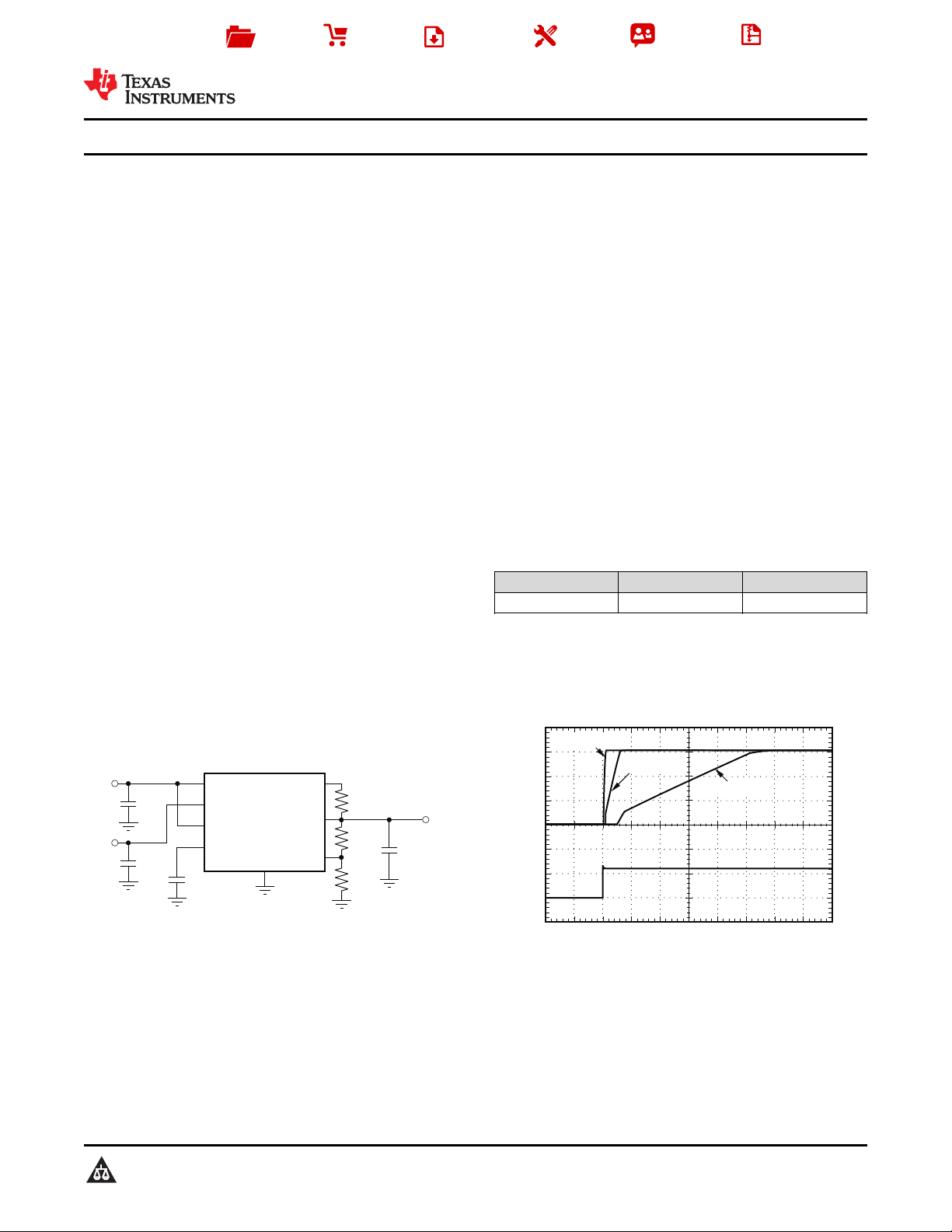
TPS74701
SBVS099G –NOVEMBER 2007–REVISED OCTOBER 2015
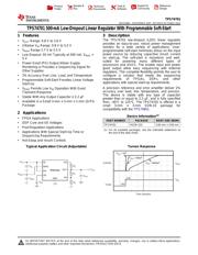
TPS74701 500-mA Low-Dropout Linear Regulator With Programmable Soft-Start
1 Features 3 Description
The TPS74701 low-dropout (LDO) linear regulator
1
• V
OUT
Range: 0.8 V to 3.6 V
provides an easy-to-use, robust power management
• Ultralow V
IN
Range: 0.8 V to 5.5 V
solution for a wide variety of applications. User-
• V
BIAS
Range 2.7 V to 5.5 V
programmable soft-start minimizes stress on the input
power source by reducing capacitive inrush current
• Low Dropout: 50 mV Typically at 500 mA, V
BIAS
=
on start-up. The soft-start is monotonic and well-
5 V
suited for powering many different types of
• Power Good (PG) Output Allows Supply
processors and ASICs. The enable input and power
Monitoring or Provides a Sequencing Signal for
good output allow easy sequencing with external
Other Supplies
regulators. This complete flexibility permits the user to
• 2% Accuracy Over Line, Load, and Temperature configure a solution that meets the sequencing
requirements of FPGAs, DSPs, and other
• Programmable Soft-Start Provides Linear Voltage
applications with special start-up requirements.
Start-Up
A precision reference and error amplifier deliver 2%
• V
BIAS
Permits Low V
IN
Operation With Good
accuracy over load, line, temperature, and process.
Transient Response
The device is stable with any type of capacitor
• Stable With Any Output Capacitor ≥ 2.2 μF
greater than or equal to 2.2 μF, and is fully specified
• Available in a Small 3-mm × 3-mm × 1-mm 10-Pin
from –40°C to 125°C. The TPS74701 is offered in a
Package
small 3-mm × 3-mm SON-10 package for
compatibility with the TPS74801.
2 Applications
Device Information
(1)
• FPGA Applications
PART NUMBER PACKAGE BODY SIZE (NOM)
• DSP Core and I/O Voltages
TPS74701 VSON (10) 3.00 mm × 3.00 mm
• Post-Regulation Applications
(1) For all available packages, see the orderable addendum at
• Applications With Special Start-Up Time or
the end of the data sheet.
Sequencing Requirements
• Hot-Swap and Inrush Controls
Typical Application Circuit (Adjustable) Turnon Response
1
An IMPORTANT NOTICE at the end of this data sheet addresses availability, warranty, changes, use in safety-critical applications,
intellectual property matters and other important disclaimers. PRODUCTION DATA.
Verzeichnis
- ・ Konfiguration des Pinbelegungsdiagramms on Seite 3
- ・ Abmessungen des Paketumrisses on Seite 23 Seite 25 Seite 26 Seite 28
- ・ Paket-Footprint-Pad-Layout on Seite 18 Seite 29
- ・ Markierungsinformationen on Seite 23
- ・ Blockdiagramm on Seite 11 Seite 15
- ・ Typisches Anwendungsschaltbild on Seite 1 Seite 15 Seite 17
- ・ Technische Daten on Seite 4
- ・ Anwendungsbereich on Seite 1
- ・ Elektrische Spezifikation on Seite 6