
herunterladen
© Semiconductor Components Industries, LLC, 2006
March, 2006 − Rev. 2
1 Publication Order Number:
SA572/D
SA572
Programmable Analog
Compandor
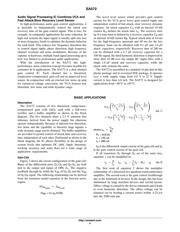
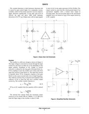
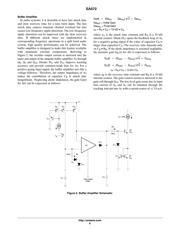
The SA572 is a dual-channel, high-performance gain control
circuit in which either channel may be used for dynamic range
compression or expansion. Each channel has a full-wave rectifier to
detect the average value of input signal, a linearized, temperature-
compensated variable gain cell (G) and a dynamic time constant
buffer. The buffer permits independent control of dynamic attack and
recovery time with minimum external components and improved low
frequency gain control ripple distortion over previous compandors.
The SA572 is intended for noise reduction in high-performance
audio systems. It can also be used in a wide range of communication
systems and video recording applications.
Features
• Independent Control of Attack and Recovery Time
• Improved Low Frequency Gain Control Ripple
• Complementary Gain Compression and Expansion with
External Op Amp
• Wide Dynamic Range − Greater than 110 dB
• Temperature-Compensated Gain Control
• Low Distortion Gain Cell
• Low Noise − 6.0 V Typical
• Wide Supply Voltage Range − 6.0 V-22 V
• System Level Adjustable with External Components
• Pb−Free Packages are Available*
Applications
• Dynamic Noise Reduction System
• Voltage Control Amplifier
• Stereo Expandor
• Automatic Level Control
• High-Level Limiter
• Low-Level Noise Gate
• State Variable Filter
*For additional information on our Pb−Free strategy and soldering details, please
download the ON Semiconductor Soldering and Mounting Techniques Reference
Manual, SOLDERRM/D.
http://onsemi.com
See detailed ordering and shipping information in the package
dimensions section on page 10 of this data sheet.
ORDERING INFORMATION
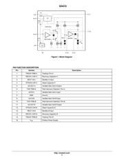
PIN CONNECTIONS
1
2
3
4
5
6
7
8
9
10
11
12
13
14
16
15
D, N, DTB Packages*
TRACK TRIM A
RECOV. CAP A
RECT. IN A
ATTACK CAP A
THD TRIM A
GND
G OUT A
G IN A
TRACK TRIM B
RECOV. CAP B
RECT. IN B
ATTACK CAP B
THD TRIM B
G OUT B
G IN B
V
CC
*D package released in large SO (SOL) package only.
PDIP−16
N SUFFIX
CASE 648
16
1
16
SOIC−16 WB
D SUFFIX
CASE 751G
1
MARKING DIAGRAMS
16
1
SA572D
AWLYYWWG
16
1
SA572N
AWLYYWWG
A = Assembly Location
WL = Wafer Lot
YY = Year
WW = Work Week
G or G = Pb−Free Package
16
1
SA
572
ALYW G
G
TSSOP−16
DTB SUFFIX
CASE 948F
16
1
http://onsemi.com
(Note: Microdot may be in either location)
Verzeichnis
- ・ Konfiguration des Pinbelegungsdiagramms on Seite 1
- ・ Abmessungen des Paketumrisses on Seite 11 Seite 12
- ・ Teilenummerierungssystem on Seite 1 Seite 10 Seite 12
- ・ Markierungsinformationen on Seite 1
- ・ Blockdiagramm on Seite 2 Seite 5 Seite 6 Seite 7 Seite 8
- ・ Beschreibung der Funktionen on Seite 2
- ・ Anwendungsbereich on Seite 1 Seite 4
- ・ Elektrische Spezifikation on Seite 3