
herunterladen
© 2007 Microchip Technology Inc. Preliminary DS41207D-page 1
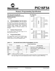
PIC16F54
This document includes the
programming specifications for the
following devices:
•PIC16F54
1.0 PROGRAMMING THE PIC16F54
The PIC16F54 is programmed using a serial method.
The Serial mode will allow the PIC16F54 to be
programmed while in the user’s system. This allows for
increased design flexibility. This programming
specification applies to PIC16F54 devices in all
packages.
1.1 Hardware Requirements
The PIC16F54 requires one power supply for VDD
(5.0V) and one for VPP (12V).
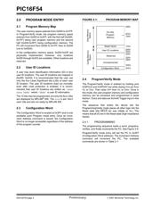
1.2 Program/Verify Mode
The Program/Verify mode for the PIC16F54 allows
programming of user program memory, special
locations used for ID, and the Configuration Word.
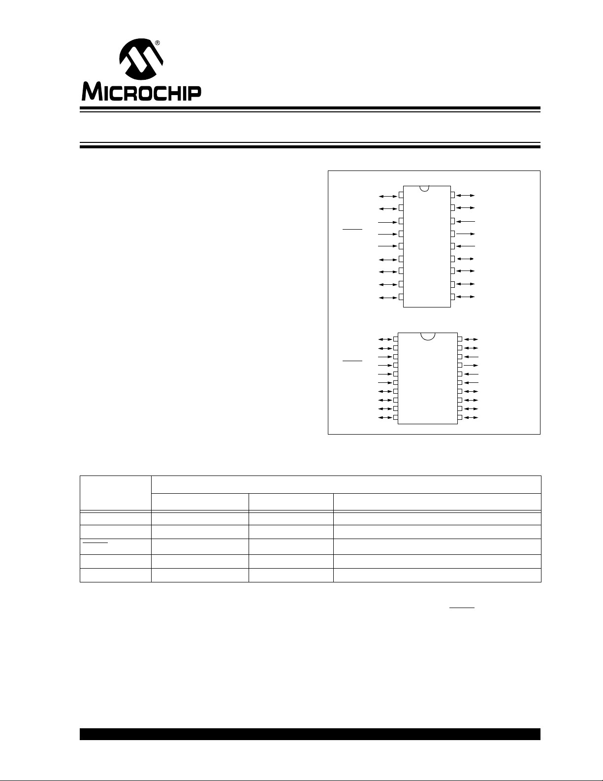
Pin Diagrams
TABLE 1-1: PIN DESCRIPTIONS (DURING PROGRAMMING): PIC16F54
PDIP, SOIC
RA1
RA0
OSC1/CLKIN
OSC2/CLKOUT
V
DD
VDD
RB7/ICSPDAT
RB6/ICSPCLK
RB5
RB4
RA2
RA3
T0CKI
MCLR
/VPP
VSS
VSS
RB0
RB1
RB2
RB3
•1
2
3
4
5
6
7
8
9
10
20
19
18
17
16
15
14
13
12
11
SSOP
RA2
RA3
T0CKI
MCLR/VPP
VSS
RB0
RB1
RB2
RB3
•1
2
3
4
5
6
7
8
9
10
18
17
16
15
14
13
12
11
RA1
RA0
OSC1/CLKIN
OSC2/CLKOUT
V
DD
RB7/ICSPDAT
RB6/ICSPCLK
RB5
RB4
PIC16F54
PIC16F54
Pin Name
During Programming
Function Pin Type Pin Description
RB6 ICSPCLK I Clock input – Schmitt Trigger input
RB7 ICSPDAT I/O Data input/output – Schmitt Trigger input
MCLR
/VPP Program/Verify mode P
(1)
Program Mode Select
VDD VDD P Power Supply
V
SS VSS P Ground
Legend: I = Input, O = Output, P = Power
Note 1: In the PIC16F54, the programming high voltage is internally generated. To activate the Program/Verify
mode, high voltage of I
IHH current capability (see Table 5-1) needs to be applied to MCLR input.
Memory Programming Specification
Verzeichnis