
herunterladen
2007-2011 Microchip Technology Inc. Advance Information DS41228F-page 1
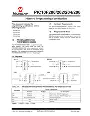
PIC10F200/202/204/206
This document includes the
programming specifications for the
following devices:
•PIC10F200
•PIC10F202
•PIC10F204
•PIC10F206
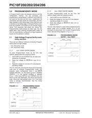
1.0 PROGRAMMING THE
PIC10F200/202/204/206
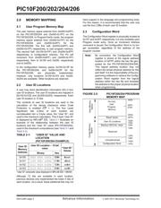
The PIC10F200/202/204/206 is programmed using a
serial method. The Serial mode will allow the
PIC10F200/202/204/206 to be programmed while in
the user’s system. This allows for increased design
flexibility. This programming specification applies to
PIC10F200/202/204/206 devices in all packages.
1.1 Hardware Requirements
The PIC10F200/202/204/206 requires one power
supply for V
DD (5.0V) and one for VPP (12V).
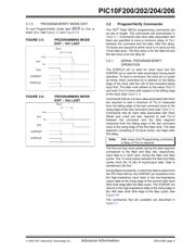
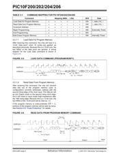
1.2 Program/Verify Mode
The Program/Verify mode for the PIC10F200/202/204/
206 allows programming of user program memory for
user ID locations, backup OSCCAL location and the
Configuration Word.
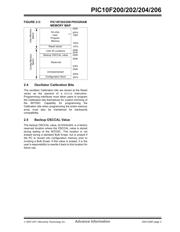
Pin Diagrams
TABLE 1-1: PIN DESCRIPTIONS (DURING PROGRAMMING): PIC10F200/202/204/206
Pin Name
During Programming
Function Pin Type Pin Description
GP1 ICSPCLK I Clock input – Schmitt Trigger input
GP0 ICSPDAT I/O Data input/output – Schmitt Trigger input
MCLR
/VPP Program/Verify mode P Programming Power
V
DD VDD P Power Supply
V
SS VSS PGround
Legend: I = Input, O = Output, P = Power
PIC10F200/2
1
2
3
6
5
4
GP0
V
SS
GP1
GP3/MCLR
/VPP
VDD
GP2/T0CKI/FOSC4
SOT-23
PIC10F204/6
1
2
3
6
5
4
GP0/CIN+
V
SS
GP1/CIN-
GP3/MCLR
/VPP
VDD
GP2/T0CKI/COUT/FOSC4
SOT-23
GP2/T0CKI/FOSC4
N/C
N/C
N/C
N/CGP2/T0CKI/COUT/FOSC4
PDIP PDIP
PIC10F200/2
1
2
3
4
8
7
6
5
VDD
GP3/MCLR/VPP
VSS
GP0
GP1
PIC10F204/6
1
2
3
4
8
7
6
5
VDD
GP3/MCLR/VPP
VSS
GP0/CIN+
GP1/CIN-
Memory Programming Specification
Verzeichnis