

herunterladen
PGA112
PGA113
PGA117
PGA116
PGA116
1
FEATURES APPLICATIONS
DESCRIPTION
10kW
ADC
G=1
R
F
R
I
Output
Stage
SPI
Interface
SCLK
DIO
CS
7
V
OUT
5
DV
DD
10
AV
DD
1
GND
6
V
REF
4
3
8
9
MSP430
Microcontroller
+3V
+5V
V
REF
PGA112
PGA113
V /CH0
CAL
2
CH1
CAL3
CAL4
CAL1
CAL2
0.1V
CAL
0.9V
CAL
10kW
80kW
MUX
CAL2/3
C
0.1 F
BYPASS
m
C
0.1 F
BYPASS
m
C
0.1 F
BYPASS
m
PGA112
, ,
PGA113
PGA116
,
PGA117
www.ti.com
............................................................................................................................................ SBOS424B – MARCH 2008 – REVISED SEPTEMBER 2008
Zer ø -Drift
PROGRAMMABLE GAIN AMPLIFIER with MUX
• Remote e-Meter Reading
23
• Rail-to-Rail Input/Output
• Automatic Gain Control
• Offset: 25 µ V (typ), 100 µ V (max)
• Portable Data Acquisition
• Zer ø Drift: 0.35 µ V/ ° C (typ), 1.2 µ V/ ° C (max)
• PC-Based Signal Acquisition Systems
• Low Noise: 12nV/ √ Hz
• Test and Measurement
• Input Offset Current: ± 5nA max (+25 ° C)
• Programmable Logic Controllers
• Gain Error: 0.1% max (G ≤ 32),
• Battery-Powered Instruments
0.3% max (G > 32)
• Handheld Test Equipment
• Binary Gains: 1, 2, 4, 8, 16, 32, 64, 128
(PGA112, PGA116)
• Scope Gains: 1, 2, 5, 10, 20, 50, 100, 200
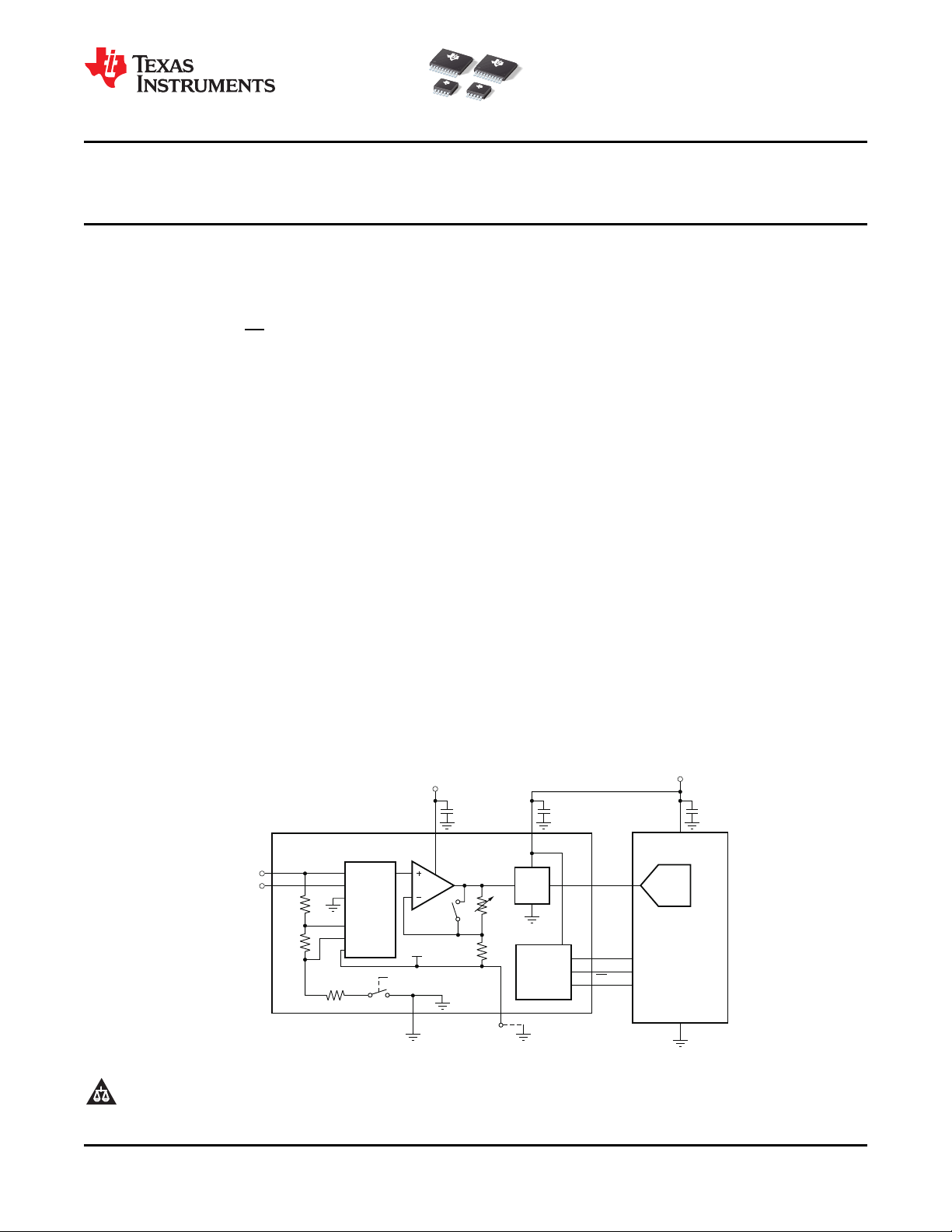
The PGA112 and PGA113 (binary/scope gains) offer
(PGA113, PGA117)
two analog inputs, a three-pin SPI interface, and
• Gain Switching Time: 200ns
software shutdown in an MSOP-10 package. The
• Two Channel MUX: PGA112, PGA113
PGA116 and PGA117 (binary/scope gains) offer 10
10 Channel MUX: PGA116, PGA117
analog inputs, a four-pin SPI interface with
daisy-chain capability, and hardware and software
• Four Internal Calibration Channels
shutdown in a TSSOP-20 package.
• Amplifier Optimized for Driving CDAC ADCs
All versions provide internal calibration channels for
• Output Swing: 50mV to Supply Rails
system-level calibration. The channels are tied to
• AV
DD
and DV
DD
for Mixed Voltage Systems
GND, 0.9V
CAL
, 0.1V
CAL
, and V
REF
, respectively. V
CAL
,
• I
Q
= 1.1mA (typ)
an external voltage connected to Channel 0, is used
as the system calibration reference. Binary gains are:
• Software/Hardware Shutdown: I
Q
≤ 4 µ A (typ)
1, 2, 4, 8, 16, 32, 64, and 128; scope gains are: 1, 2,
• Temperature Range: – 40 ° C to +125 ° C
5, 10, 20, 50, 100, and 200.
• SPI™ Interface (10MHz) with Daisy-Chain
Capability
1
Please be aware that an important notice concerning availability, standard warranty, and use in critical applications of Texas
Instruments semiconductor products and disclaimers thereto appears at the end of this data sheet.
2 SPI is a trademark of Motorola.
3 All other trademarks are the property of their respective owners.
PRODUCTION DATA information is current as of publication date.
Copyright © 2008, Texas Instruments Incorporated
Products conform to specifications per the terms of the Texas
Instruments standard warranty. Production processing does not
necessarily include testing of all parameters.
Verzeichnis