
herunterladen
© Semiconductor Components Industries, LLC, 2014
May, 2014 − Rev. 26
1 Publication Order Number:
NCP302/D
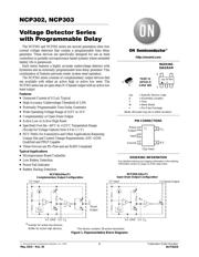
NCP302, NCP303
Voltage Detector Series
with Programmable Delay
The NCP302 and NCP303 series are second generation ultra−low
current voltage detectors that contain a programmable time delay
generator. These devices are specifically designed for use as reset
controllers in portable microprocessor based systems where extended
battery life is paramount.
Each series features a highly accurate undervoltage detector with
hysteresis and an externally programmable time delay generator. This
combination of features prevents erratic system reset operation.
The NCP302 series consists of complementary output devices that
are available with either an active high or active low reset. The
NCP303 series has an open drain N−Channel output with an active low
reset output.
Features
• Quiescent Current of 0.5 mA Typical
• High Accuracy Undervoltage Threshold of 2.0%
• Externally Programmable Time Delay Generator
• Wide Operating Voltage Range of 0.8 V to 10 V
• Complementary or Open Drain Output
• Active Low or Active High Reset
• Specified Over the −40°C to +125°C Temperature Range
(Except for Voltage Options from 0.9 to 1.1 V)
• NCV Prefix for Automotive and Other Applications Requiring
Unique Site and Control Change Requirements; AEC−Q100
Qualified and PPAP Capable
• These Devices are Pb−Free and are RoHS Compliant
Typical Applications
• Microprocessor Reset Controller
• Low Battery Detection
• Power Fail Indicator
• Battery Backup Detection
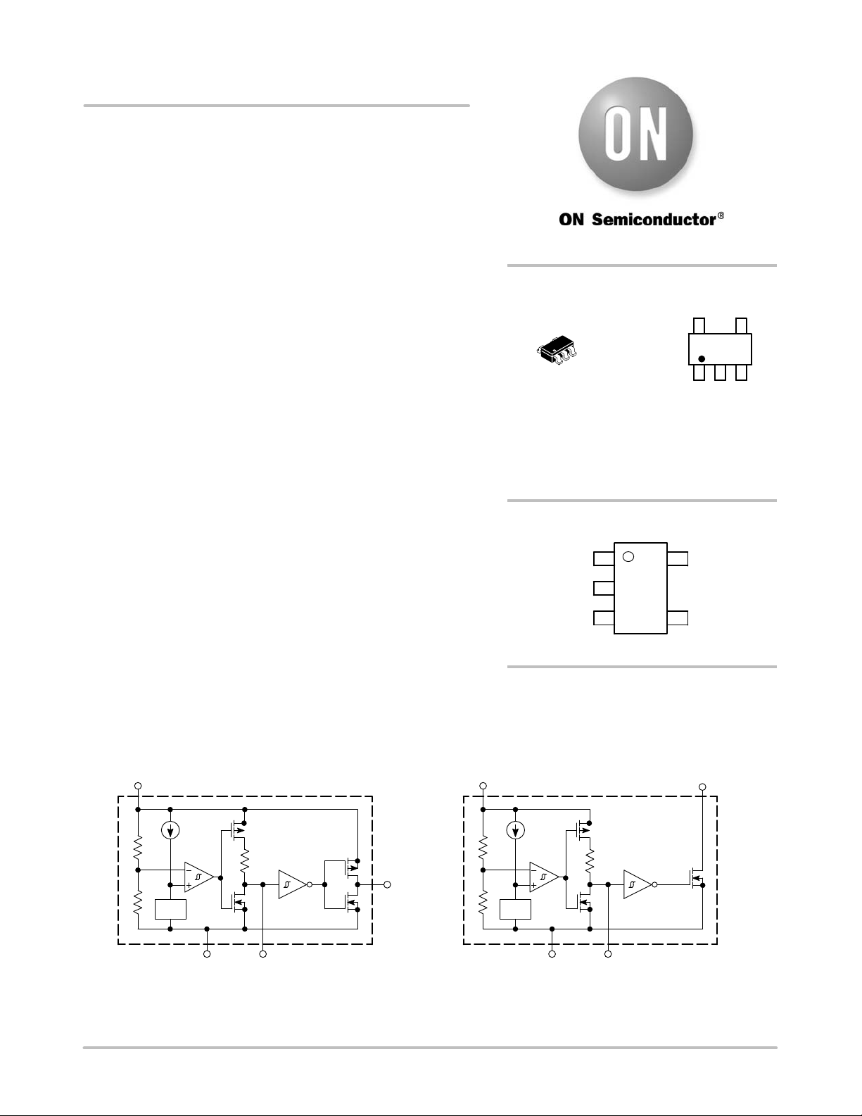
Figure 1. Representative Block Diagrams
This device contains 28 active transistors.
NCP303LSNxxT1
Open Drain Output Configuration
NCP302xSNxxT1
Complementary Output Configuration
* Inverter for active low devices.
* Buffer for active high devices.
V
ref
2 Input
1
Reset
Output
3 GND
5C
D
R
D
*
V
ref
2 Input
3 GND
5C
D
R
D
1 Reset Outp
ut
See detailed ordering and shipping information in the ordering
information section on page 22 of this data sheet.
ORDERING INFORMATION
TSOP−5/
SOT23−5
CASE 483
PIN CONNECTIONS
1
3
N.C.
Reset
Output
2
Input
Ground
4
C
D
5
(Top View)
http://onsemi.com
1
5
xxx AYWG
G
MARKING
DIAGRAM
xxx = Specific Device Code
A = Assembly Location
Y = Year
W = Work Week
G = Pb−Free Package
1
5
(Note: Microdot may be in either location)
Verzeichnis
- ・ Konfiguration des Pinbelegungsdiagramms on Seite 1
- ・ Abmessungen des Paketumrisses on Seite 26
- ・ Paket-Footprint-Pad-Layout on Seite 26
- ・ Teilenummerierungssystem on Seite 1 Seite 22 Seite 23 Seite 24 Seite 25
- ・ Markierungsinformationen on Seite 1 Seite 22 Seite 23 Seite 24 Seite 25
- ・ Blockdiagramm on Seite 1
- ・ Typisches Anwendungsschaltbild on Seite 1
- ・ Technische Daten on Seite 22 Seite 23 Seite 24 Seite 25
- ・ Anwendungsbereich on Seite 1 Seite 22 Seite 23 Seite 24 Seite 25
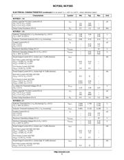
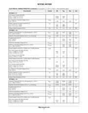
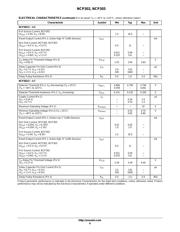
- ・ Elektrische Spezifikation on Seite 3 Seite 4 Seite 5 Seite 6
- ・ Teilenummernliste on Seite 2