
herunterladen
© Semiconductor Components Industries, LLC, 2013
May, 2013 − Rev. 7
1 Publication Order Number:
MC14569B/D
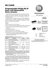
MC14569B
Programmable Divide-By-N
Dual 4-Bit Binary/BCD
Down Counter
The MC14569B is a programmable divide−by−N dual 4−bit binary
or BCD down counter constructed with MOS P−Channel and
N−Channel enhancement mode devices (complementary MOS) in a
monolithic structure.
This device has been designed for use with the MC14568B phase
comparator/counter in frequency synthesizers, phase−locked loops,
and other frequency division applications requiring low power
dissipation and/or high noise immunity.
Features
• Speed−up Circuitry for Zero Detection
• Each 4−Bit Counter Can Divide Independently in BCD or Binary Mode
• Can be Cascaded With MC14526B for Frequency Synthesizer
Applications
• All Outputs are Buffered
• Schmitt Triggered Clock Conditioning
• These Devices are Pb−Free and are RoHS Compliant
• NLV Prefix for Automotive and Other Applications Requiring
Unique Site and Control Change Requirements; AEC−Q100
Qualified and PPAP Capable
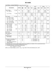
MAXIMUM RATINGS (Voltages Referenced to V
SS
)
Symbol
Parameter Value Unit
V
DD
DC Supply Voltage Range −0.5 to +18.0 V
V
in
, V
out
Input or Output Voltage Range
(DC or Transient)
−0.5 to V
DD
+ 0.5 V
I
in
, I
out
Input or Output Current
(DC or Transient) per Pin
±10 mA
P
D
Power Dissipation, per Package
(Note 1)
500 mW
T
A
Ambient Temperature Range −55 to +125 °C
T
stg
Storage Temperature Range −65 to +150 °C
T
L
Lead Temperature
(8−Second Soldering)
260 °C
Stresses exceeding Maximum Ratings may damage the device. Maximum
Ratings are stress ratings only. Functional operation above the Recommended
Operating Conditions is not implied. Extended exposure to stresses above the
Recommended Operating Conditions may affect device reliability.
1. Temperature Derating:
Plastic “P and D/DW” Packages: – 7.0 mW/_C From 65_C To 125_C
This device contains protection circuitry to guard against damage due to high
static voltages or electric fields. However, precautions must be taken to avoid
applications of any voltage higher than maximum rated voltages to this
high−impedance circuit. For proper operation, V
in
and V
out
should be constrained
to the range V
SS
v (V
in
or V
out
) v V
DD
.
Unused inputs must always be tied to an appropriate logic voltage level
(e.g., either V
SS
or V
DD
). Unused outputs must be left open.
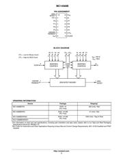
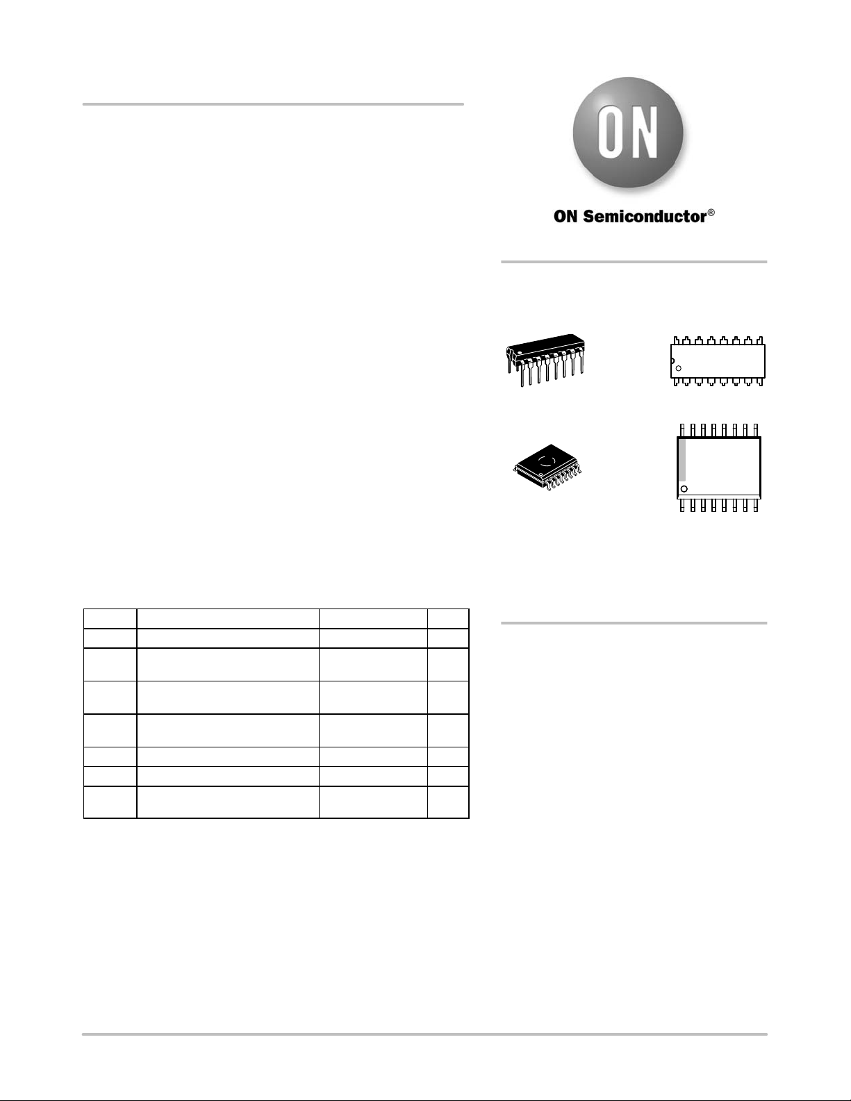
http://onsemi.com
MARKING
DIAGRAMS
PDIP−16
P SUFFIX
CASE 648
MC14569BCP
AWLYYWWG
SOIC−16 WB
DW SUFFIX
CASE 751G
A = Assembly Location
WL = Wafer Lot
YY = Year
WW = Work Week
G = Pb−Free Package
See detailed ordering and shipping information in the package
dimensions section on page 2 of this data sheet.
ORDERING INFORMATION
16
1
14569B
AWLYYWWG
16
1
Verzeichnis
- ・ Konfiguration des Pinbelegungsdiagramms on Seite 2 Seite 5
- ・ Abmessungen des Paketumrisses on Seite 12 Seite 13
- ・ Paket-Footprint-Pad-Layout on Seite 13
- ・ Teilenummerierungssystem on Seite 1 Seite 2 Seite 13
- ・ Markierungsinformationen on Seite 1 Seite 13
- ・ Blockdiagramm on Seite 2
- ・ Typisches Anwendungsschaltbild on Seite 10 Seite 11
- ・ Technische Daten on Seite 2
- ・ Anwendungsbereich on Seite 1 Seite 2 Seite 11
- ・ Elektrische Spezifikation on Seite 3