
herunterladen
LTC3114-1
1
31141fa
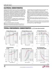
For more information www.linear.com/LTC3114-1
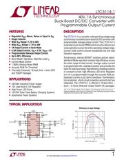
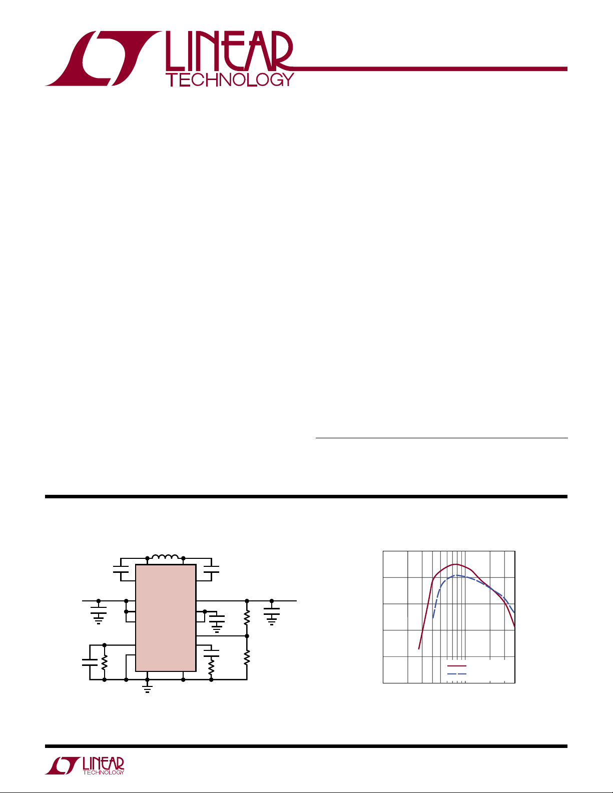
TYPICAL APPLICATION
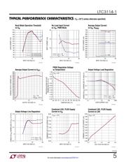
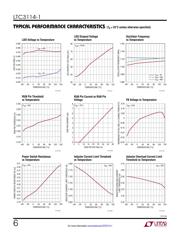
FEATURES DESCRIPTION
40V, 1A Synchronous
Buck-Boost DC/DC Converter with
Programmable Output Current
The LTC
®
3114-1 is a versatile, wide operating voltage range
synchronous monolithic buck-boost DC/DC converter with
programmable average output current. The LTC3114-1’s
proprietary buck-boost PWM control circuitry delivers low
noise operation across the entire operating voltage range.
Current mode control ensures exceptional line and load
transient responses.
Synchronous, internal MOSFET switches and pin select
-
able Burst
Mode operation maintain high efficiency across
the
entire range of load current. Average output current
is programmed with a standard resistor and provides the
basis for wide input range, high efficiency charging systems
or constant current, high efficiency LED drive. Regulator
turn-on is programmable through the accurate RUN pin.
Quiescent current is just 3µA in shutdown. Overtempera
-
ture protection,
short-circuit protection and soft-start are
integrated. The LTC3114-1 is offered in 16-lead 3mm ×
5mm × 0.75mm DFN and 16 lead TSSOP (FE) packages.
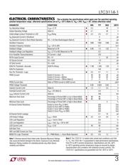
Efficiency vs Input Voltage
APPLICATIONS
n
Regulates V
OUT
Above, Below or Equal to V
IN
n
Single Inductor
n
Wide V
IN
Range: 2.2V to 40V
n
Wide V
OUT
Range: 2.7V to 40V
n
1A Output Current in Buck Mode
n
0.5A Output Current, V
IN
= 3.6V, V
OUT
= 5V
n
Programmable Average Output Current
n
Up to 96% Efficiency
n
Burst Mode
®
Operation, 30µA No-Load I
Q
n
Current Mode Control
n
1.2MHz Ultralow Noise PWM
n
Accurate RUN Pin Threshold
n
Thermally Enhanced, 16-lead 3mm × 5mm DFN
and TSSOP Packages
n
24V/28V Industrial Power Supply
n
12V Lead-Acid to 12V Regulator
n
High Power LED Driver
n
12V/24V Solar Panel Battery Charging Systems
n
Automotive Power Systems
L, LT, LTC, LTM, Burst Mode, LTspice, µModule, Linear Technology and the Linear logo are
registered trademarks and No R
SENSE
is a trademark of Linear Technology Corporation. All other
trademarks are the property of their respective owners.
6.8µH
SW1 SW2
GND PGND
BST1
68nF
4.7µF
4700pF
27.4k
499k
31141 TA01a
2M
20k33nF
68nF
BST2
V
IN
PV
OUT
PV
IN
LDO
PLDO
FB
RUN
10µF
V
IN
2.7V TO 40V
VCPROG
MODE
30µF
V
OUT
5V
1A
V
IN
> 5V
LTC3114-1
INPUT VOLTAGE (V)
EFFICIENCY (%)
95
90
85
31141 TA01b
70
80
75
1 10 40
I
LOAD
= 300mA
I
LOAD
= 600mA
Verzeichnis
- ・ Konfiguration des Pinbelegungsdiagramms on Seite 9 Seite 10
- ・ Abmessungen des Paketumrisses on Seite 31
- ・ Paket-Footprint-Pad-Layout on Seite 32
- ・ Blockdiagramm on Seite 8 Seite 11 Seite 23
- ・ Typisches Anwendungsschaltbild on Seite 1 Seite 20 Seite 27 Seite 28 Seite 29
- ・ Technische Daten on Seite 3
- ・ Anwendungsbereich on Seite 1 Seite 9 Seite 12 Seite 19 Seite 20
- ・ Elektrische Spezifikation on Seite 3 Seite 4 Seite 5 Seite 6 Seite 7