
herunterladen
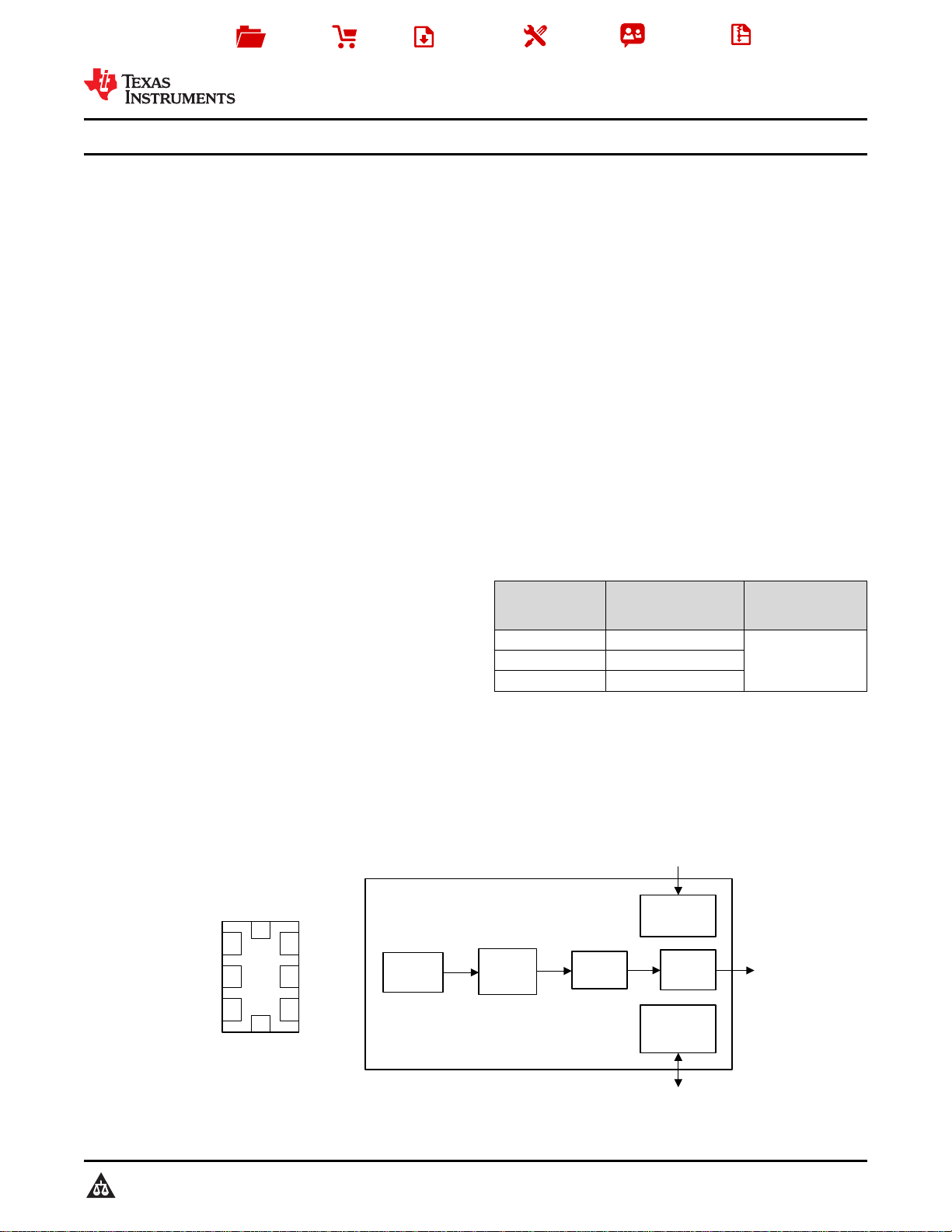
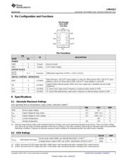
ADD OUTN
VDDOE
GND OUTP
SCL
SDA
1 6
2 5
43
7
8
LMK61E2
Ultra-high performance oscillator
PLL
Output
Divider
Output
Buffer
Power
Conditioning
Interface
I
2
C/EEPROM
Integrated
Oscillator
Copyright © 2016, Texas Instruments Incorporated
Product
Folder
Order
Now
Technical
Documents
Tools &
Software
Support &
Community
Reference
Design
An IMPORTANT NOTICE at the end of this data sheet addresses availability, warranty, changes, use in safety-critical applications,
intellectual property matters and other important disclaimers. PRODUCTION DATA.
LMK61E2
SNAS674B –SEPTEMBER 2015–REVISED FEBRUARY 2017
LMK61E2 Ultra-Low Jitter Programmable Oscillator With Internal EEPROM
1
1 Features
1
• Ultra-Low Noise, High Performance
– Jitter: 90 fs RMS Typical f
OUT
> 100 MHz
– PSRR: –70 dBc, Robust Supply Noise
Immunity
• Flexible Output Format; User Selectable
– LVPECL up to 1 GHz
– LVDS up to 900 MHz
– HCSL up to 400 MHz
• Total Frequency Tolerance of ±50 ppm
• System Level Features
– Frequency Margining: Fine and Coarse
– Internal EEPROM: User Configurable Default
Settings
• Other Features
– Device Control: I
2
C
– 3.3-V Operating Voltage
– Industrial Temperature Range (–40ºC to
+85ºC)
– 7-mm × 5-mm 8-Pin Package
– Create a Custom Design Using the LMK61E2
With the WEBENCH
®
Power Designer
2 Applications
• High-Performance Replacement for Crystal-,
SAW-, or Silicon-Based Oscillators
• Switches, Routers, Network Line Cards, Base
Band Units (BBU), Servers, Storage/SAN
• Test and Measurement
• Medical Imaging
• FPGA, Processor Attach
3 Description
The LMK61E2 device is an ultra-low jitter
PLLatinum™ programmable oscillator with a
fractional-N frequency synthesizer with integrated
VCO that generates commonly used reference
clocks. The outputs can be configured as LVPECL,
LVDS, or HCSL.
The device features self start-up from on-chip
EEPROM that is factory programmed to generate
156.25-MHz LVPECL output. The device registers
and EEPROM settings are fully programmable in-
system through I
2
C serial interface. Internal power
conditioning provide excellent power supply ripple
rejection (PSRR), reducing the cost and complexity of
the power delivery network. The device operates from
a single 3.3-V ± 5% supply.
The device provides fine and coarse frequency
margining options through I
2
C serial interface to
support system design verification tests (DVT), such
as standard compliance and system timing margin
testing.
Device Information
(1)
PART NUMBER
DEFAULT OUTPUT
FREQ (MHz) AND
FORMAT
PACKAGE AND
BODY SIZE (NOM)
LMK61E2 156.25 LVPECL
8-pin QFM (SIA),
7.00 mm x 5.00 mm
LMK61E2BAA 156.25 LVDS
LMK61E2BBA 125 LVDS
(1) For all available packages, see the orderable addendum at
the end of the data sheet.
Pinout and Simplified Block Diagram
Verzeichnis
- ・ Konfiguration des Pinbelegungsdiagramms on Seite 3
- ・ Abmessungen des Paketumrisses on Seite 48 Seite 50 Seite 51 Seite 52
- ・ Paket-Footprint-Pad-Layout on Seite 45 Seite 53
- ・ Markierungsinformationen on Seite 48
- ・ Blockdiagramm on Seite 1 Seite 14
- ・ Typisches Anwendungsschaltbild on Seite 37 Seite 38 Seite 39 Seite 40 Seite 41
- ・ Schweißen Temperatur on Seite 44
- ・ Technische Daten on Seite 3
- ・ Anwendungsbereich on Seite 1 Seite 37 Seite 38 Seite 39 Seite 40
- ・ Elektrische Spezifikation on Seite 4