

herunterladen
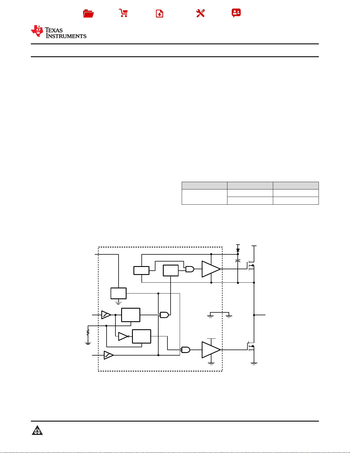
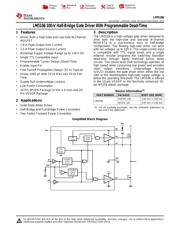
LO
DRIVER
V
DD
UVLO
HO
DRIVER
HB
UVLO
LEVEL
SHIFT
HB
HS
IN
EN
LEADING
EDGE
DELAY
LEADING
EDGE
DELAY
RDT
V
DD
V
DD
V
DD
V
SS
Product
Folder
Sample &
Buy
Technical
Documents
Tools &
Software
Support &
Community
LM5106
SNVS424D –JANUARY 2006–REVISED DECEMBER 2014
LM5106 100-V Half-Bridge Gate Driver With Programmable Dead-Time
1 Features 3 Description
The LM5106 is a high-voltage gate driver designed to
1
• Drives Both a High-Side and Low-Side N-Channel
drive both the high-side and low-side N-channel
MOSFET
MOSFETs in a synchronous buck or half-bridge
• 1.8-A Peak Output Sink Current
configuration. The floating high-side driver can work
• 1.2-A Peak Output Source Current
with rail voltages up to 100 V. The single control input
is compatible with TTL signal levels and a single
• Bootstrap Supply Voltage Range up to 118-V DC
external resistor programs the switching transition
• Single TTL Compatible Input
dead-time through tightly matched turnon delay
• Programmable Turnon Delays (Dead-Time)
circuits. The robust level shift technology operates at
high speed while consuming low power and provides
• Enable Input Pin
clean output transitions. Undervoltage lockout
• Fast Turnoff Propagation Delays (32 ns Typical)
(UVLO) disables the gate driver when either the low
• Drives 1000 pF With 15-ns Rise and 10-ns Fall
side or the bootstrapped high-side supply voltage is
Time
below the operating threshold. The LM5106 is offered
in the 10-pin VSSOP or the thermally enhanced 10-
• Supply Rail Undervoltage Lockout
pin WSON plastic package.
• Low Power Consumption
• 10-Pin WSON Package (4 mm × 4 mm) and 10-
Device Information
(1)
Pin VSSOP Package
PART NUMBER PACKAGE BODY SIZE (NOM)
VSSOP (10) 3.00 mm × 3.00 mm
2 Applications
LM5106
WSON (10) 4.00 mm × 4.00 mm
• Solid-State Motor Drives
(1) For all available packages, see the orderable addendum at
• Half-Bridge and Full-Bridge Power Converters
the end of the datasheet.
• Two Switch Forward Power Converters
Simplified Block Diagram
1
An IMPORTANT NOTICE at the end of this data sheet addresses availability, warranty, changes, use in safety-critical applications,
intellectual property matters and other important disclaimers. PRODUCTION DATA.
Verzeichnis
- ・ Konfiguration des Pinbelegungsdiagramms on Seite 3
- ・ Abmessungen des Paketumrisses on Seite 18 Seite 20 Seite 21
- ・ Markierungsinformationen on Seite 18
- ・ Blockdiagramm on Seite 1 Seite 11
- ・ Typisches Anwendungsschaltbild on Seite 12 Seite 13
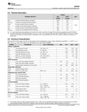
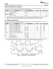
- ・ Technische Daten on Seite 4
- ・ Anwendungsbereich on Seite 1 Seite 26
- ・ Elektrische Spezifikation on Seite 4 Seite 5 Seite 6