

herunterladen
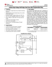
DRIVER
DRIVER
LEVEL
SHIFT
UVLO
UVLO
HI
V
DD
LI
V
SS
HB
HO
HS
LO
HV
Adjustable
rising
edge delay
RT2
RT1
Adjustable
rising
edge delay
Product
Folder
Sample &
Buy
Technical
Documents
Tools &
Software
Support &
Community
LM5102
SNVS268B –MAY 2004–REVISED DECEMBER 2014
LM5102 High-Voltage Half-Bridge Gate Driver With Programmable Delay
1 Features 3 Description
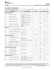
The LM5102 high-voltage gate driver is designed to
1
• Drives Both a High-Side and Low-Side N-Channel
drive both the high side and the low side N-Channel
MOSFET
MOSFETs in a synchronous buck or a half bridge
• Independently Programmable High and Low Side
configuration. The floating high-side driver is capable
Rising Edge Delay
of working with supply voltages up to 100 V. The
outputs are independently controlled. The rising edge
• Bootstrap Supply Voltage Range up to 118 V dc
of each output can be independently delayed with a
• Fast Turn-Off Propagation Delay (25 ns Typical)
programming resistor. An integrated high voltage
• Drives 1000-pF Loads with 15-ns Rise and Fall
diode is provided to charge the high side gate drive
Times
bootstrap capacitor. A robust level shifter operates at
• Supply Rail Undervoltage Lockout high speed while consuming low power and providing
clean level transitions from control logic to the high
• Low Power Consumption
side gate driver. Undervoltage lockout is provided on
• Timer Can Be Terminated Midway Through
both the low side and the high side power rails. This
Sequence
device is available in the standard VSSOP 10 pin and
the WSON 10 pin packages.
2 Applications
Device Information
(1)
• Current Fed Push-Pull Power Converters
PART NUMBER PACKAGE BODY SIZE (NOM)
• Half and Full Bridge Power Converters
VSSOP (10) 3.00 mm × 3.00 mm
• Synchronous Buck Converters
LM5102
WSON (10) 4.00 mm × 4.00 mm
• Two Switch Forward Power Converters
(1) For all available packages, see the orderable addendum at
• Forward with Active Clamp Converters
the end of the data sheet.
Simplified Block Diagram
1
An IMPORTANT NOTICE at the end of this data sheet addresses availability, warranty, changes, use in safety-critical applications,
intellectual property matters and other important disclaimers. PRODUCTION DATA.
Verzeichnis
- ・ Konfiguration des Pinbelegungsdiagramms on Seite 3
- ・ Abmessungen des Paketumrisses on Seite 16 Seite 18 Seite 19
- ・ Markierungsinformationen on Seite 16
- ・ Blockdiagramm on Seite 1 Seite 10
- ・ Typisches Anwendungsschaltbild on Seite 11 Seite 12
- ・ Technische Daten on Seite 4 Seite 5 Seite 6
- ・ Anwendungsbereich on Seite 1 Seite 22
- ・ Elektrische Spezifikation on Seite 5 Seite 6