
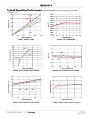
1
DATASHEET
High Performance 1A Linear Regulator with
Programmable Current Limiting
ISL80101A
The ISL80101A is a low dropout voltage, single output LDO
with programmable current limiting. This LDO operates from
input voltages of 2.2V to 6V, and is capable of providing output
voltages of 0.8V to 5V. Other custom voltage options are
available upon request.
A submicron BiCMOS process is utilized for this product family
to deliver the best-in-class analog performance and overall
value. The programmable current limiting improves system
reliability of end applications. An external capacitor on the
soft-start pin provides an adjustable soft-starting ramp. The
ENABLE feature allows the part to be placed into a low
quiescent current shutdown mode.
This CMOS LDO will consume significantly lower quiescent
current as a function of load compared to bipolar LDOs, which
translates into higher efficiency and packages with smaller
footprints. Quiescent current is modestly compromised to
achieve a very fast load transient response.
Table 1
shows the differences between the ISL80101A and
others in its family:
Features
• ±2% V
ADJ
accuracy guaranteed over line, load and
T
J
= -40°C to +125°C
• Very low 212mV dropout voltage at V
IN
= 4.5V
• High accuracy current limit programmable up to 1.75A
• Very fast transient response
• 100µV
RMS
output noise
• Power-good output
•Programmable soft-start
• Over-temperature protection
•Small 10 Ld DFN package
Applications
• Telecommunications and networking
• Medical equipment
• Instrumentation systems
•USB devices
•Gaming
•Routers and switchers
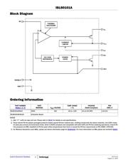
TABLE 1. KEY DIFFERENCES BETWEEN FAMILY OF PARTS
PART NUMBER
PROGRAMMABLE
I
LIMIT
I
LIMIT
(DEFAULT)
ADJ or FIXED
V
OUT
ISL80101-ADJ No 1.75A ADJ
ISL80101 No 1.75A 1.8V, 2.5V,
3.3V, 5.0V
ISL80101A Yes 1.62A ADJ
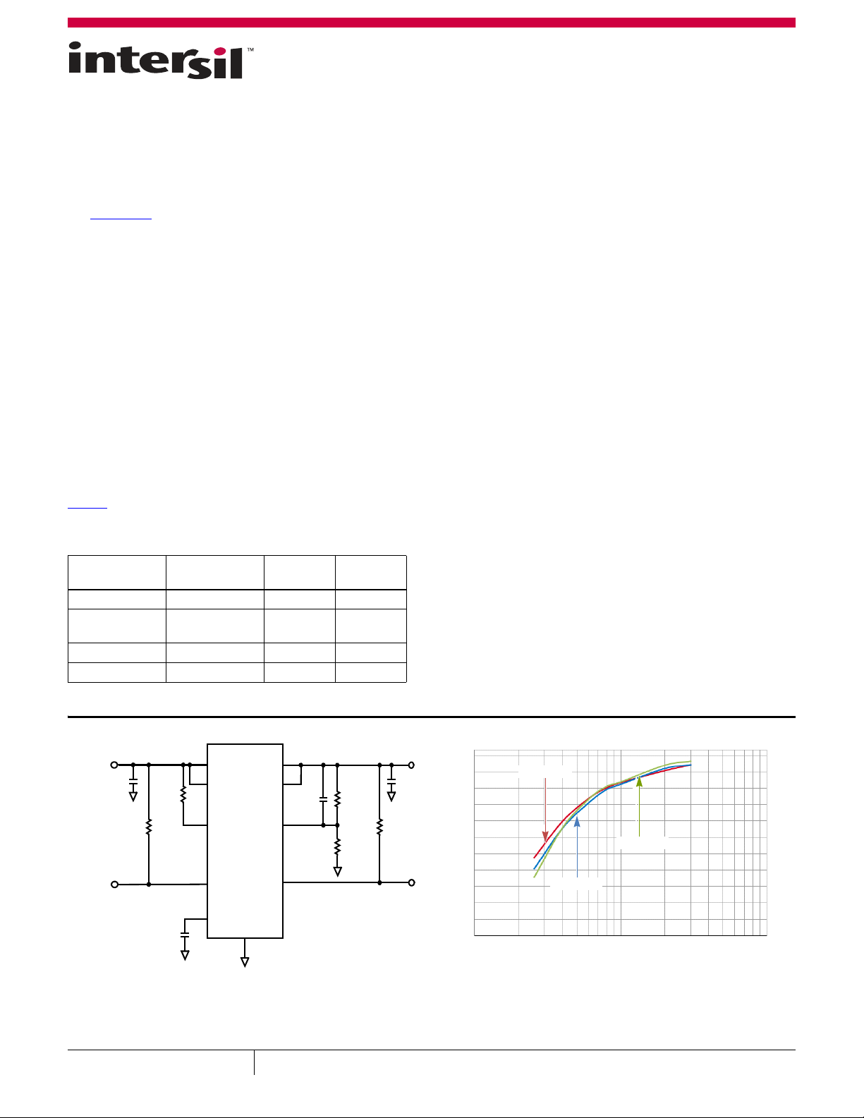
ISL80121-5 Yes 0.75A 5.0V
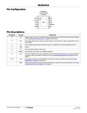
V
IN
PGENABLE
SS
GND
V
IN
1
2
5
4
7
10
9
6
10k
100k
10µF
5.0V ± 5%
3.3V
ADJ
2.61k
0.464k
ISL80101A
C
SS
C
PB
C
OUT
R
1
0.01µF
R
3
R
2
100pF
3
8
I
SET
R
SET
10µF
C
IN
I
LIMIT
1.62
2.9x2xV
IN
1–
R
SET
k
----------------------------------------
–~
V
OUT
V
OUT
FIGURE 1. TYPICAL APPLICATION
R
SET
(kΩ)
CURRENT LIMIT (A)
V
IN
= 5.0V
V
IN
= 5.5V
V
IN
= 4.5V
10 100 1000
1.5
1.2
0.9
0.6
0.3
0.0
August 11, 2015
FN7712.4
CAUTION: These devices are sensitive to electrostatic discharge; follow proper IC Handling Procedures.
1-888-INTERSIL or 1-888-468-3774
| Copyright Intersil Americas LLC 2010, 2011, 2015. All Rights Reserved
Intersil (and design) is a trademark owned by Intersil Corporation or one of its subsidiaries.
All other trademarks mentioned are the property of their respective owners.
Verzeichnis
- ・ Konfiguration des Pinbelegungsdiagramms on Seite 3
- ・ Abmessungen des Paketumrisses on Seite 13
- ・ Teilenummerierungssystem on Seite 2
- ・ Markierungsinformationen on Seite 2
- ・ Blockdiagramm on Seite 2
- ・ Typisches Anwendungsschaltbild on Seite 1
- ・ Beschreibung der Funktionen on Seite 5 Seite 8
- ・ Technische Daten on Seite 5
- ・ Anwendungsbereich on Seite 1 Seite 5
- ・ Elektrische Spezifikation on Seite 5