
herunterladen
iCE40
™
LP Series
Ultra Low-Power
mobileFPGA
™
Family
March 30, 2012 (1.31)
Data Sheet
© 2007-2012 by Lattice Semiconductor Corporation. All rights reserved. (1.31, 30-MAR-2012)
www.latticesemi.com 1
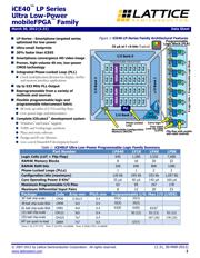
LP-Series - Smartphone targeted series
optimized for low power
Ultra-small footprints
30% faster than iCE65
Smartphone convergence HD video image
Proven, high-volume 40 nm, low-power
CMOS technology
Integrated Phase-Locked Loop (PLL)
Clock multiplication/division for display, SerDes
and memory interface applications
Up to 533 MHz PLL Output
Reprogrammable from a variety of
methods and sources
Flexible programmable logic and
programmable interconnect fabric
8K look-up tables (LUT4) and flip-flops
Low-power logic and interconnect
Complete iCEcube2
™
development system
Windows
®
and Linux
®
support
VHDL and Verilog logic synthesis
Place and route software
Design and IP core libraries
Low-cost iCEman40LP development board
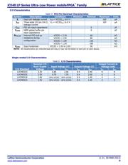
Table 1:
iCE40LP Ultra Low-Power Programmable Logic Family Summary
Part Number
LP640
LP1K
LP4K
LP8K
Logic Cells (LUT + Flip-Flop)
640
1,280
3,520
7,680
RAM4K Memory Blocks
8
16
20
32
RAM4K RAM bits
32K
64K
80K
128K
Phase-Locked Loops (PLLs)
1
1
2
2
Configuration bits (maximum)
120 Kb
245 Kb
533 Kb
1,057 Kb
Core Operating Power 0 KHz
1
35 µA
40 µA
140 µA
160 µA
Maximum Programmable I/O Pins
63
95
167
178
Maximum Differential Input Pairs
8
12
20
23
Package
Code
Area mm
Pitch mm
Programmable I/O: Max I/O (LVDS)
36
2
-ball chip-scale
BGA
CM36
2.5x2.5
0.4
25(3)
25(3)
49-ball chip-scale BGA
CM49
3x3
0.4
35(5)
35(5)
81-ball chip-scale BGA
CM81
4x4
0.4
63(8)
63(8)
63(9)
3
121-ball chip-scale
BGA
CM121
5x5
0.4
95 (12)
93 (13)
93 (13)
225-ball chip-scale
BGA
CM225
7x7
0.4
167 (20)
178 (23)
84
2
-pin quad no-lead
packall chip-scale BGA
QN84
7x7
0.5
67(7)
Note 1: At 1.2V VCC Note 2: No PLL Available Note 3: Only 1 PLL Available
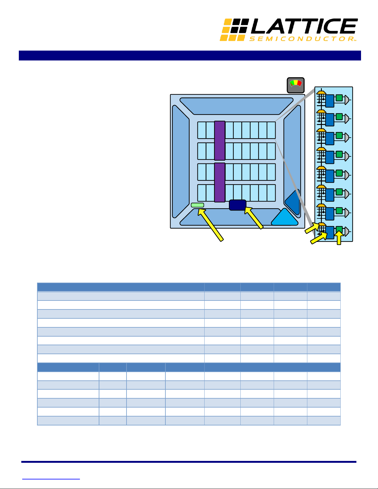
Figure 1:
iCE40 LP-Series Family Architectural Features
I/O Bank 0
I/O Bank 2
I/O Bank 1
I/O Bank 3
PLB
PLB
PLB
PLB
PLB
PLB
PLBPLBPLB
PLBPLBPLB
PLBPLBPLB
Programmable Interconnect
Programmable Interconnect
35 µA at f =0 kHz (Typical)
NVCM
PLBPLBPLB
4Kbit RAM 4Kbit RAM
PLBPLBPLBPLB
Nonvolatile Configuration
Memory (NVCM)
PLBPLBPLBPLB
JTAG
Four-input
Look-Up Table
(LUT4)
Carry logic
Flip-flop with enable
and reset controls
Programmable
Logic Block (PLB)
8 Logic Cells = Programmable Logic Block
PLB
PLB
PLB
PLB
Programmable Interconnect
PLB
PLB
SPI
Config
PLL
Phase-Locked
Loop
Verzeichnis