
herunterladen

PSoC
®
5LP: CY8C52LP Family
Datasheet
Programmable System-on-Chip (PSoC
®
)
Cypress Semiconductor Corporation • 198 Champion Court • San Jose, CA 95134-1709 • 408-943-2600
Document Number: 001-84933 Rev. *J Revised October 25, 2016
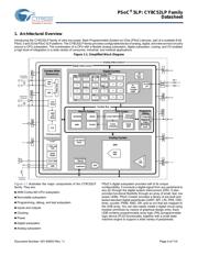
General Description
PSoC
®
5LP is a true programmable embedded system-on-chip, integrating configurable analog and digital peripherals, memory, and
a microcontroller on a single chip. The PSoC 5LP architecture boosts performance through:
32-bit ARM Cortex-M3 core plus DMA controller at up to 80 MHz
Ultra low power with industry’s widest voltage range
Programmable digital and analog peripherals enable custom functions
Flexible routing of any analog or digital peripheral function to any pin
PSoC devices employ a highly configurable system-on-chip architecture for embedded control design. They integrate configurable
analog and digital circuits, controlled by an on-chip microcontroller. A single PSoC device can integrate as many as 100 digital and
analog peripheral functions, reducing design time, board space, power consumption, and system cost while improving system quality.
Features
Operating characteristics
Voltage range: 1.71 to 5.5 V, up to 6 power domains
Temperature range (ambient) –40 to 85 °C
[1]
DC to 80-MHz operation
Power modes
• Active mode 3.1 mA at 6 MHz, and 15.4 mA at 48 MHz
• 2-µA sleep mode
• 300-nA hibernate mode with RAM retention
Boost regulator from 0.5-V input up to 5-V output
Performance
32-bit ARM Cortex-M3 CPU, 32 interrupt inputs
24-channel direct memory access (DMA) controller
Memories
Up to 256 KB program flash, with cache and security features
Up to 32 KB additional flash for error correcting code (ECC)
Up to 64 KB RAM
2 KB EEPROM
Digital peripherals
Four 16-bit timer, counter, and PWM (TCPWM) blocks
I
2
C, 1 Mbps bus speed
USB 2.0 certified Full-Speed (FS) 12 Mbps peripheral inter-
face (TID#10840032) using internal oscillator
[2]
20 to 24 universal digital blocks (UDB), programmable to
create any number of functions:
• 8-, 16-, 24-, and 32-bit timers, counters, and PWMs
•I
2
C, UART, SPI, I2S, LIN 2.0 interfaces
• Cyclic redundancy check (CRC)
• Pseudo random sequence (PRS) generators
• Quadrature decoders
• Gate-level logic functions
Programmable clocking
3- to 74-MHz internal oscillator, 2% accuracy at 3 MHz
4- to 25-MHz external crystal oscillator
Internal PLL clock generation up to 80 MHz
Low-power internal oscillator at 1, 33, and 100 kHz
32.768-kHz external watch crystal oscillator
12 clock dividers routable to any peripheral or I/O
Analog peripherals
12-bit SAR ADC
8-bit DAC
Two comparators
CapSense
®
support, up to 62 sensors
1.024 V ±1% internal voltage reference
Versatile I/O system
46 to 72 I/O pins – up to 62 general-purpose I/Os (GPIOs)
Up to eight performance I/O (SIO) pins
• 25 mA current sink
• Programmable input threshold and output high voltages
• Can act as a general-purpose comparator
• Hot swap capability and overvoltage tolerance
Two USBIO pins that can be used as GPIOs
Route any digital or analog peripheral to any GPIO
LCD direct drive from any GPIO, up to 46 × 16 segments
CapSense support from any GPIO
1.2-V to 5.5-V interface voltages, up to four power domains
Programming, debug, and trace
JTAG (4-wire), serial wire debug (SWD) (2-wire), single wire
viewer (SWV), and Traceport (5-wire) interfaces
ARM debug and trace modules embedded in the CPU core
Bootloader programming through I
2
C, SPI, UART, USB, and
other interfaces
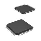
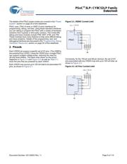
Package options: 68-pin QFN,100-pin TQFP, and 99-pin CSP
Development support with free PSoC Creator™ tool
Schematic and firmware design support
Over 100 PSoC Components™ integrate multiple ICs and
system interfaces into one PSoC. Components are free
embedded ICs represented by icons. Drag and drop
component icons to design systems in PSoC Creator.
Includes free GCC compiler, supports Keil/ARM MDK
compiler
Supports device programming and debugging
Notes
1. The maximum storage temperature is 150 °C in compliance with JEDEC Standard JESD22-A103, High Temperature Storage Life.
2. This feature on select devices only. See Ordering Information on page 104 for details.
Verzeichnis
- ・ Konfiguration des Pinbelegungsdiagramms on Seite 11 Seite 47 Seite 80
- ・ Abmessungen des Paketumrisses on Seite 107
- ・ Teilenummerierungssystem on Seite 1 Seite 104 Seite 105
- ・ Blockdiagramm on Seite 1 Seite 4 Seite 10 Seite 13 Seite 21
- ・ Schweißen Temperatur on Seite 106
- ・ Beschreibung der Funktionen on Seite 1 Seite 23 Seite 42 Seite 50 Seite 52
- ・ Technische Daten on Seite 38 Seite 47 Seite 60 Seite 61 Seite 62
- ・ Anwendungsbereich on Seite 28
- ・ Elektrische Spezifikation on Seite 47 Seite 60
- ・ Teilenummernliste on Seite 60