
herunterladen
PRELIMINARY
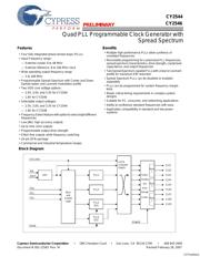
Quad PLL Programmable Clock Generator with
Spread Spectrum
CY2546
CY2544
Cypress Semiconductor Corporation • 198 Champion Court • San Jose, CA 95134-1709 • 408-943-2600
Document #: 001-12563 Rev. *A Revised February 28, 2007
Features
• Four fully integrated phase-locked loops (PLLs)
• Input Frequency range:
— External crystal: 8 to 48 MHz
— External reference: 8 to 166 MHz clock
• Wide operating output frequency range
— 3 to 166 MHz
• Programmable Spread Spectrum with Center and Down
Spread option and Lexmark modulation profile
• Two VDD core voltage options:
— 2.5V, 3.0V, and 3.3V for CY2544
— 1.8V for CY2546
• Selectable output voltages:
— 2.5V, 3.0V, and 3.3V for CY2544
— 1.8V for CY2546
• Frequency Select feature with option to select eight different
frequencies
• Low jitter, high accuracy outputs
• Up to nine clock outputs
• Programmable output drive strength
• Glitch-free outputs while frequency switching
• 24-pin QFN package
• Commercial and Industrial temperature ranges
Benefits
• Multiple high-performance PLLs allow synthesis of
unrelated frequencies
• Nonvolatile programming for customized PLL frequencies,
spread spectrum characteristics, drive strength, crystal load
capacitance, and output frequencies
• Two Spread Spectrum capable PLLs with Linear or Lexmark
profile for maximum EMI reduction
• Spread Spectrum PLLs can be disabled or enabled
separately
• PLLs can be programmed for system frequency margin
tests
• Meets critical timing requirements in complex system
designs
• Suitable for PC, consumer, and networking applications
• Ability to synthesize standard frequencies with ease
• Application compatibility in standard and low-power
systems
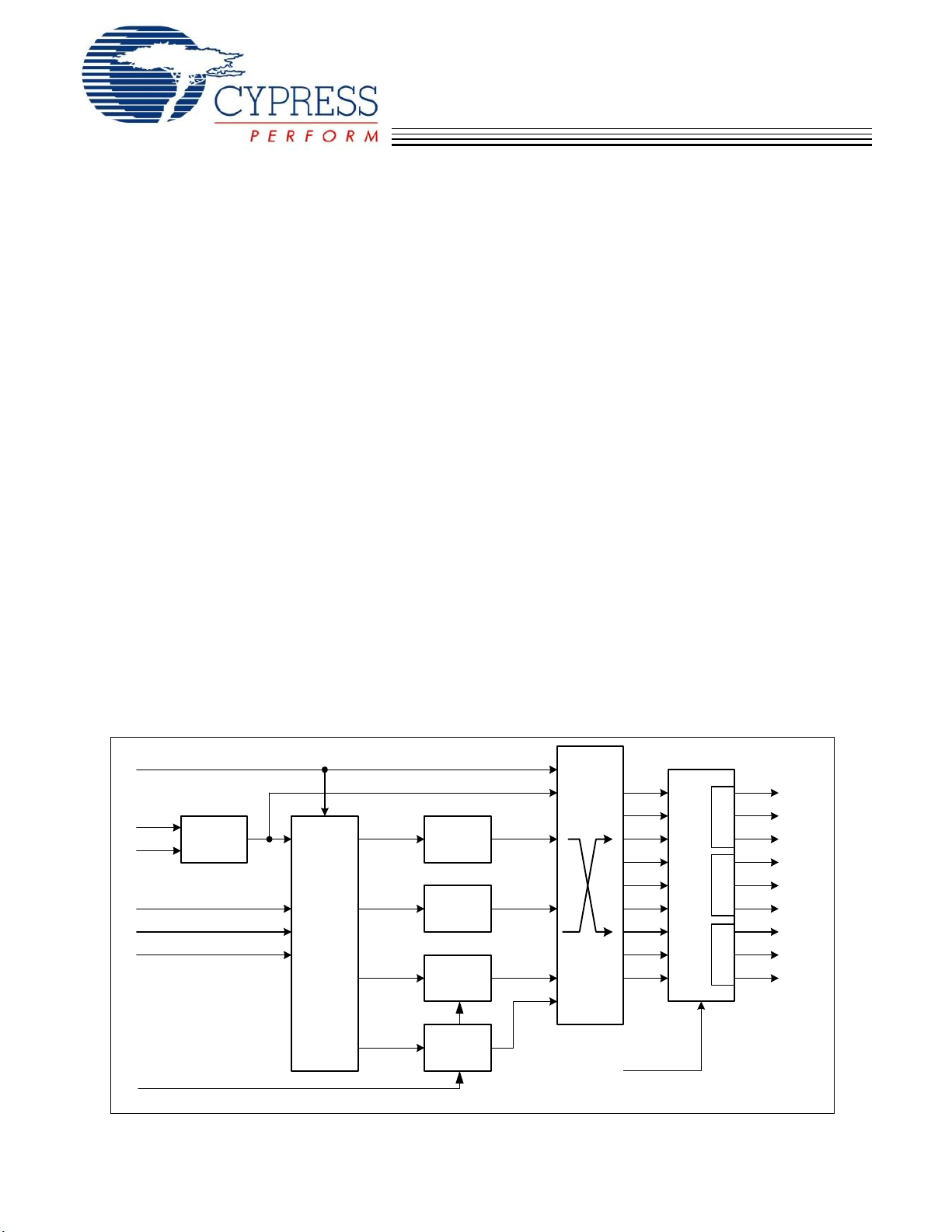
Block Diagram
OSC
MUX
and
Control
Logic
PLL1
PLL2
PLL3
(SS)
PLL4
(SS)
Output
Dividers
and
Drive
Strength
Control
CLK1
CLK9
CLK8
CLK7
CLK6
CLK5
CLK4
CLK3
CLK2
4of6
Crossbar
Switch
EXCLKIN
FS2
FS1
FS0
SSON
XOUT
XIN
PD#/OE
Bank
1
Bank
3
Bank
2
[+] Feedback
Verzeichnis