
herunterladen
1
FEATURES
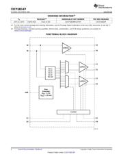
V
SS
(
2)
S0
V
DD
1
Y1
Y1
V
DD
1
V
SS
18
17
16
15
14
13
1
2
3
4
5
6
EN
V
DD
PECL
IN
IN
V
DD
PECL
VBB
24 23 22 21 20 19
7 8 9 10 11 12
S2
V
DD
0
Y0
Y0
V
DD
0
S1
V
SS
V
DD
2
Y2
Y2
V
DD
2
NC
RGE PACKAGE
(TOP VIEW)
(2)
Thermal pad must be connected to V
SS
.
P0024-02
SUPPORTS DEFENSE, AEROSPACE,
DESCRIPTION/ORDERING INFORMATION
CDCP1803-EP
www.ti.com
........................................................................................................................................................................................... SCAS864 – DECEMBER 2008
1:3 LVPECL CLOCK BUFFER WITH PROGRAMMABLE DIVIDER
• Distributes One Differential Clock Input to
Three LVPECL Differential Clock Outputs
• Programmable Output Divider for Two LVPECL
Outputs
• Low-Output Skew 15 ps (Typical)
• V
CC
Range 3 V – 3.6 V
• Signaling Rate Up to 800-MHz LVPECL
• Differential Input Stage for Wide
Common-Mode Range
• Provides VBB Bias Voltage Output for
Single-Ended Input Signals
• Receiver Input Threshold ± 75 mV
• 24-Terminal QFN Package (4 mm × 4 mm)
• Accepts Any Differential Signaling:
LVDS, HSTL, CML, VML, SSTL-2, and
Single-Ended: LVTTL/LVCMOS
AND MEDICAL APPLICATIONS
• Controlled Baseline
• One Assembly/Test Site
• One Fabrication Site
• Available in Military ( – 55 ° C/125 ° C)
Temperature Range
(1)
• Extended Product Life Cycle
• Extended Product-Change Notification
• Product Traceability
(1) Additional temperature ranges available - contact factory
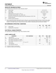
The CDCP1803 clock driver distributes one pair of differential clock inputs to three pairs of LVPECL differential
clock outputs Y[2:0] and Y[2:0] with minimum skew for clock distribution. The CDCP1803 is specifically designed
for driving 50- Ω transmission lines.
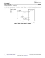
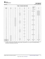
The CDCP1803 has three control terminals, S0, S1, and S2, to select different output mode settings; see Table 1
for details. The CDCP1803 is characterized for operation from – 55 ° C to 125 ° C. For use in single-ended driver
applications, the CDCP1803 also provides a VBB output terminal that can be directly connected to the unused
input as a common-mode voltage reference.
1
Please be aware that an important notice concerning availability, standard warranty, and use in critical applications of Texas
Instruments semiconductor products and disclaimers thereto appears at the end of this data sheet.
PRODUCTION DATA information is current as of publication date.
Copyright © 2008, Texas Instruments Incorporated
Products conform to specifications per the terms of the Texas
Instruments standard warranty. Production processing does not
necessarily include testing of all parameters.
Verzeichnis