

herunterladen
Digitally Programmable
Sensor Signal Amplifier
Data Sheet
AD8557
Rev. D Document Feedback
Information furnished by Analog Devices is believed to be accurate and reliable. However, no
responsibility is assumed by Analog Devices for its use, nor for any infringements of patents or other
rights of third parties that may result from its use. Specifications subject to change without notice. No
license is granted by implication or otherwise under any patent or patent rights of Analog Devices.
Trademarks and registered trademarks are the property of their respective owners.
One Technology Way, P.O. Box 9106, Norwood, MA 02062-9106, U.S.A.
Tel: 781.329.4700 ©2007–2016 Analog Devices, Inc. All rights reserved.
Technical Support www.analog.com
FEATURES
Very low offset voltage: 12 μV maximum over temperature
Very low input offset voltage drift: 65 nV/°C maximum
High CMRR: 96 dB minimum
Digitally programmable gain and output offset voltage
Gain range from 28 to 1300
Qualified for automotive applications
Single-wire serial interface
Stable with any capacitive load
SOIC and LFCSP packages
2.7 V to 5.5 V operation
APPLICATIONS
Automotive sensors
Pressure and position sensors
Precision current sensing
Thermocouple amplifiers
Industrial weigh scales
Strain gages
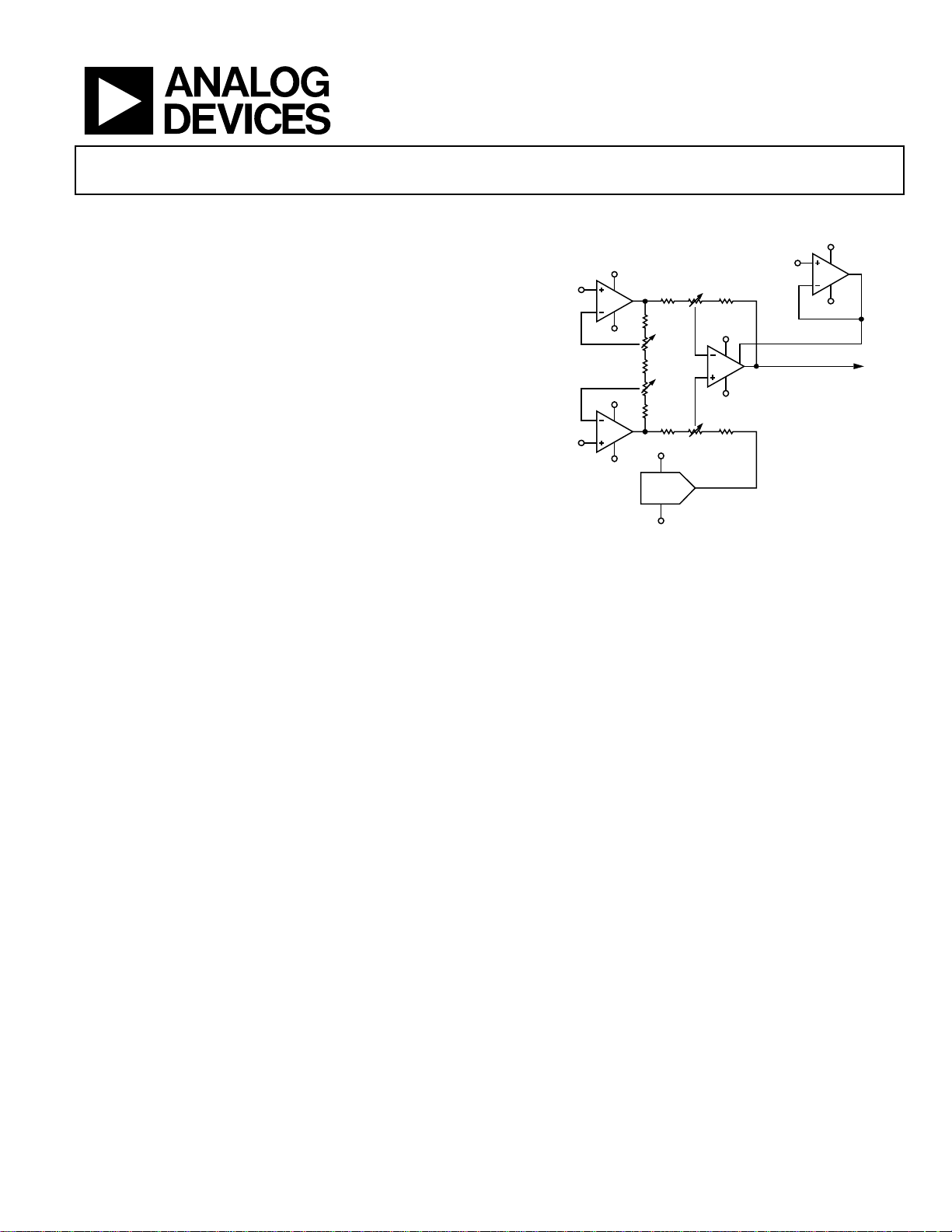
FUNCTIONAL BLOCK DIAGRAM
A3
A2
A4
VDD
VDD
DIGIN
VSS
VSS
VDD
VSS
V
DD
VCLAMP
VPOS
VSS
V
OU
T
A1
VDD
VSS
VNEG
R1
R3
R2
R5 R7
P4
R4
R6
P3
P2
P1
06013-001
Figure 1.
GENERAL DESCRIPTION
The AD8557 is a zero drift, sensor signal amplifier with digitally
programmable gain and output offset. Designed to easily and
accurately convert variable pressure sensor and strain bridge
outputs to a well-defined output voltage range, the AD8557
accurately amplifies many other differential or single-ended
sensor outputs. The AD8557 uses the Analog Devices, Inc.,
proprietary low noise auto-zero and DigiTrim® technologies to
create an accurate and flexible signal processing solution in a
compact footprint.
Gain is digitally programmable in a wide range from 28 to 1300
through a serial data interface. Gain adjustment can be fully
simulated in circuit and then permanently programmed with
reliable polyfuse technology. Output offset voltage is also digitally
programmable and is ratiometric to the supply voltage.
In addition to extremely low input offset voltage and input
offset voltage drift and very high dc and ac CMRR, the AD8557
also includes a pull-up current source at the input pins and a
pull-down current source at the VCLAMP pin. Output clamping
set via an external reference voltage allows the AD8557 to drive
lower voltage analog-to-digital converters (ADCs) safely and
accurately.
When used in conjunction with an ADC referenced to the same
supply, the system accuracy becomes immune to normal supply
voltage variations. Output offset voltage can be adjusted with a
resolution of better than 0.4% of the difference between VDD
and VSS. A lockout trim after gain and offset adjustment
further ensures field reliability.
The AD8557 is fully specified from −40°C to +125°C.
Operating from single-supply voltages of 2.7 V to 5.5 V, the
AD8557 is offered in an 8-lead SOIC, and a 4 mm × 4 mm,
16-lead LFCSP.
Verzeichnis
- ・ Konfiguration des Pinbelegungsdiagramms on Seite 6 Seite 21
- ・ Abmessungen des Paketumrisses on Seite 21
- ・ Teilenummerierungssystem on Seite 22
- ・ Blockdiagramm on Seite 1 Seite 14
- ・ Beschreibung der Funktionen on Seite 1 Seite 6 Seite 21
- ・ Technische Daten on Seite 1 Seite 3 Seite 5 Seite 17 Seite 22
- ・ Anwendungsbereich on Seite 1
- ・ Elektrische Spezifikation on Seite 7