
herunterladen
Si501/2/3/4
LVCMOS CMEMS
®
Programmable Oscillator Series
Revision 0.72 Copyright© 2013 by Silicon Labs Si501/2/3/4 CMEMS Oscillator Series
www.silabs.com/cmems
This information applies to a product under development. Its characteristics and specifications are subject to change without notice.
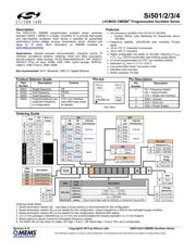
Description
The Si501/2/3/4 CMEMS programmable oscillator series combines
standard CMOS + MEMS in a single, monolithic IC to provide high-quality
and high-reliability oscillators. Each device is specified for guaranteed
performance across voltage, process, temperature, shock, vibration and
aging for 10 years. More information on CMEMS available at
www.silabs.com/cmems.
Applications: General purpose microcontrollers, industrial control, IP
cameras, surveillance systems, metering, home and office automation,
security systems, sleep clocking, 10/100 Ethernet/EtherCAT, SPI, SAS3.0 /
SATA3.0, PCIe ref clock, NVMe, HDD, SSD, hybrid storage, DDR3/3L,
USB2.0, USB OTG/2.0, M2M, HDMI
Not recommended: Wi-Fi, Bluetooth, USB 3.0, Gigabit Ethernet
Features
Any frequency oscillator from 32 kHz to 100 MHz
o Contact Silicon Labs Marketing for frequencies above
100 MHz
Frequency stability: ±20/±30/±50 ppm including 10-year
aging
-20 to +70 °C: Extended Commercial
-40 to +85 °C: Industrial
Highly configurable: low power vs. low jitter, frequency, F
STAB
,
T
R
/T
F
, V
DD
, OE/FS functionality (see ordering guide below)
In-circuit programmable via C1D 1-pin interface (Si504)
Seamless V
DD
from +1.71 to +3.63 V
Low period jitter mode / low power mode
Glitchless start and stop
RoHS compliant, Pb-free
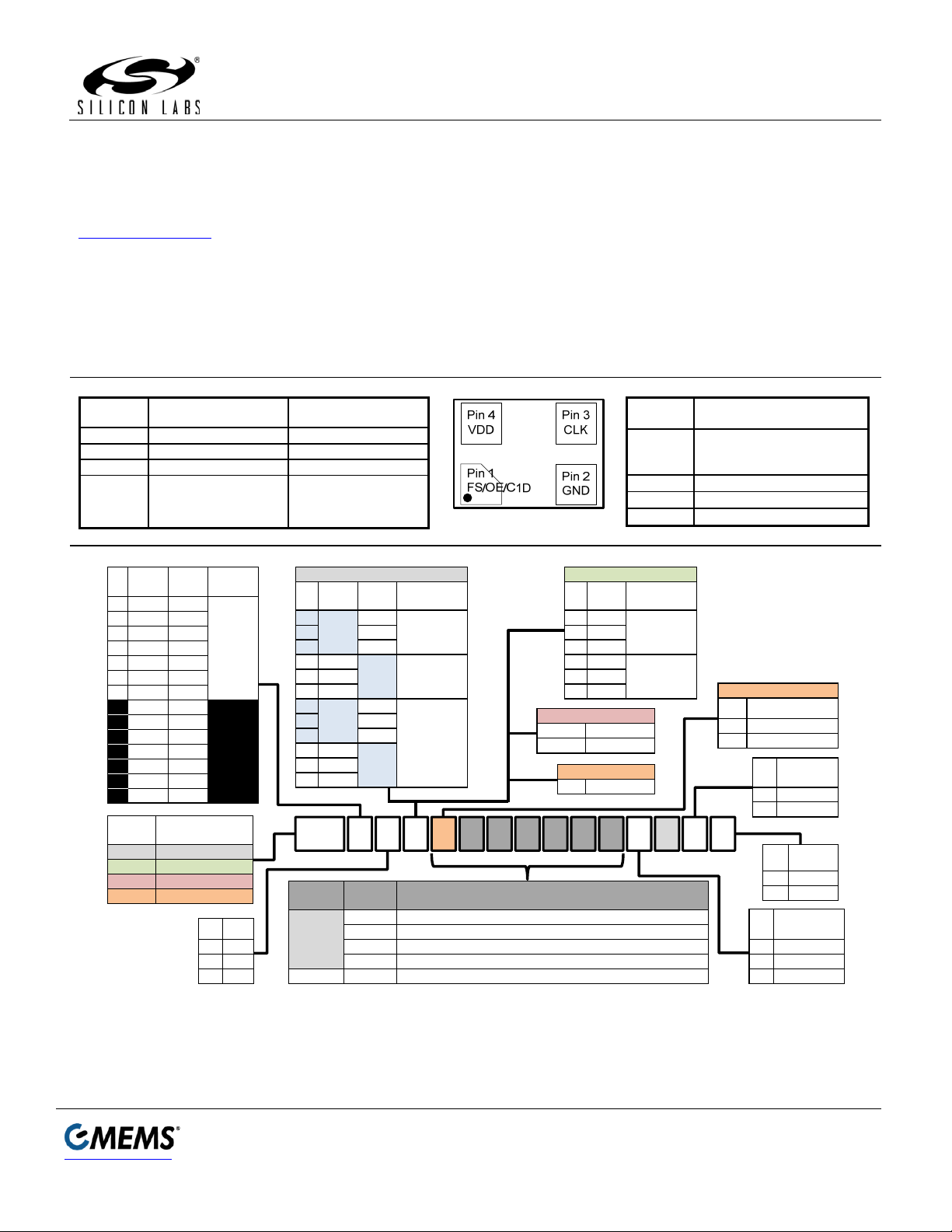
Product Selector Guide
Part
Number
Description Control
Si501 Single frequency OE
Si502 Dual frequency FS/OE
Si503 Quad frequency FS
Si504 Programmable for any
supported frequency
or configuration
C1D 1-pin interface
(see Si504 data sheet
for details)
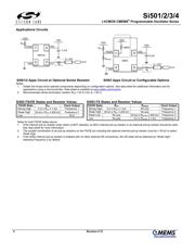
Pin-out
(top view)
Pin Description
Pin
Number
Description
1 FS = Frequency Select
OE = Output Enable
C1D = Single wire interface
2 GND = Ground
3 CLK = Clock out
4 VDD = Power Supply
Ordering Guide
Ordering Guide Notes:
1. Series termination resistor (R
S
– see Apps Circuits section) is recommended for this configuration.
2. Series termination resistor (R
S
) is not needed for this configuration. Output impedance is 50Ω for the indicated supply condition.
3. Series termination resistor (R
S
) is not needed for this configuration. Reduced EMI setting.
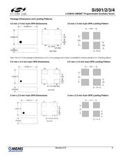
4. 3.2 x 5 mm package is delivered as 3.2 x 4 mm and accommodates the industry-standard 3.2 x 5 mm footprint.
5. Select option to support maximum anticipated frequency needed.
6. The Si502 OE pin has three (3) states: OE High = Freq 1; OE Weak High = Freq 2; OE Low is configurable.
50X ‐ ‐ ‐ ‐ ‐ ‐ ‐ ‐ ‐ ‐ A ‐
ppm
A ±50
B ±30
C ±20
Package
Dimension
B 3.2x5mm
4
C 2.5x3.2mm
D 2x2.5mm
R
Temp
Range
F ‐20to70°C
G ‐40to85°C
Reel
R Reel
CutTape
OPN
Freq
Code
Description
501only
Mxxxxxx f
OUT
<1MHz
xMxxxxx 1MHz≤f
OUT
<10MHz
xxMxxxx 10MHz≤f
OUT
<100MHz
100M000 f
OUT
=100MHz
501/2/3/4 xxxxxx SiliconLabs6‐digitcodefor502/3/4,or>6‐decimalfreq on501
501
OE
High
OE
Low
Internal
PullResistor
A
Enable
Stop
Pull‐UpB Doze
C Sleep
D Stop
Enable Pull‐DownE Doze
F Sleep
G
Enable
Stop
None
H Doze
J Sleep
K Stop
EnableL Doze
M Sleep
VDD
TYP
T
R
/T
F
Jittervs
Power
A 1.7‐3.6 0.7ns
1
Low
Power
B 3.3V 1.3ns
2
C 2.5V 1.3ns
2
D 1.8V 1.3ns
2
E 1.7‐3.6 3ns
3
F 1.7‐3.6 5ns
3
G 1.7‐3.6 8ns
3
H 1.7‐3.6 0.7ns
1
Low Jitter
J 3.3V 1.3ns
2
K 2.5V 1.3ns
2
L 1.8V 1.3ns
2
M 1.7‐3.6 3ns
3
N 1.7‐3.6 5ns
3
P 1.7‐3.6 8ns
3
OPN
Prefix
Description
501 Singlefrequency
502 Dual frequency
503 Quad frequency
504 Anyfrequency
502
6
OE
Low
Internal
PullResistor
A Stop
Pull‐UpB Do ze
C Sleep
D Stop
NoneE Doze
F Sleep
503
A Pull‐Up
B None
504
A Pull‐Uponly
‐
504only
5
Maximum F
OUT
A 0.032–80MHz
B 0.032– 100MHz
Verzeichnis
- ・ Konfiguration des Pinbelegungsdiagramms on Seite 1
- ・ Abmessungen des Paketumrisses on Seite 1 Seite 3 Seite 5
- ・ Paket-Footprint-Pad-Layout on Seite 5
- ・ Teilenummerierungssystem on Seite 1
- ・ Markierungsinformationen on Seite 6
- ・ Technische Daten on Seite 2
- ・ Anwendungsbereich on Seite 1 Seite 4
- ・ Elektrische Spezifikation on Seite 2