
herunterladen
1
Microsemi Corporation
Copyright 2014, Microsemi Corporation. All Rights Reserved.
Features
Inputs/Outputs
• Accepts two differential or single-ended inputs
• LVPECL, LVDS, CML, HCSL, LVCMOS
•
Glitch-free switching of references
• On-chip input termination and biasing for AC
couple
d inputs
• Eight precision LVDS outputs
• Operating frequency up to 750 MHz
Power
• Option for 2.5 V or 3.3 V power supply
• Current consumption of 114 mA
• On-chip Low Drop Out (LDO) Regulator for superior
power su
pply rejection
Performance
• Ultra low additive jitter of 165 fs RMS
Applications
• General purpose clock distribution
• Low jitter clock trees
• Logic translation
• Clock and data signal restoration
• Redundant clock distribution
• Wired communications: OTN, SONET/SDH, GE,
10 GE, FC and 10G FC
• PCI Express generation 1/2/3 clock distribution
• Wireless communications
• High performance microprocessor clock
distribution
April 2014
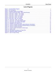
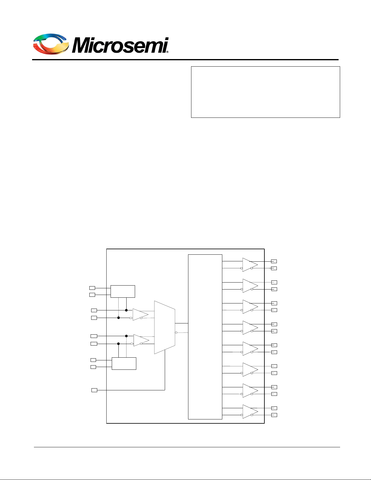
Figure 1 - Functional Block Diagram
clk0_p
clk0_n
ctrl0
vt0
sel
Termination
and Bias
clk1_p
clk1_n
ctrl1
vt1
Termination
and Bias
Control
out6_p
out6_n
out5_p
out5_n
out7_p
out7_n
out4_p
out4_n
out3_p
out3_n
out2_p
out2_n
out1_p
out1_n
out0_p
out0_n
Buffer
ZL40223
Precision 2:8 LVDS Fanout Buffer with Glitch-
free Input Reference Switching
and On-Chip Input Termination
Data Sheet
Ordering Information
ZL40223LDG1 32 Pin QFN Trays
ZL40223LDF1 32 Pin QFN Tape and Reel
Matte Tin
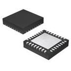
Package size: 5 x 5 mm
-40
o
C to +85
o
C
Verzeichnis
- ・ Konfiguration des Pinbelegungsdiagramms on Seite 4 Seite 6
- ・ Teilenummerierungssystem on Seite 1
- ・ Blockdiagramm on Seite 1
- ・ Beschreibung der Funktionen on Seite 1 Seite 4 Seite 5 Seite 6 Seite 7
- ・ Technische Daten on Seite 18
- ・ Anwendungsbereich on Seite 1 Seite 4
- ・ Elektrische Spezifikation on Seite 18 Seite 19