
herunterladen

Application Note Please read the Important Notice and Warnings at the end of this document V3.5
www.infineon.com 2016-02-22
AP24026
EMC and System-ESD Design Guidelines for
Board Layout
About this document
Scope and purpose
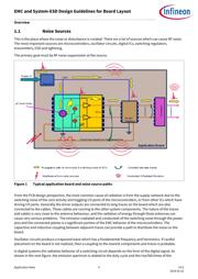
This document provides information for EMC optimized PCB design and system ESD design. The topics covered
include PCB Design considerations regarding the routing of high speed signals, selecting stack-up of the PCB,
selecting decoupling components, impedance controlled design of the traces, and termination of high speed
signal paths. Special considerations for microcontrollers are also provided.
Attention:
This application note contains design recommendations from Infineon Technologies point of
view. Effectiveness and performance of the final application implementation must be
validated by the customer, based on their specific implementation choices.
Intended audience
This document is intended for anyone who needs to design EMC optimized application boards using
microcontrollers and other components from Infineon Technologies AG.
Table of Contents
About this document ......................................................................................................................... 1
Table of Contents .............................................................................................................................. 1
1 Overview ........................................................................................................................ 3
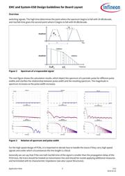
1.1 Noise Sources .......................................................................................................................................... 4
1.2 Coupling paths ........................................................................................................................................ 6
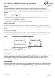
1.2.1 Common-mode and differential-mode ............................................................................................. 6
2 PCB considerations .......................................................................................................... 9
3 Design measures .............................................................................................................12
3.1 Power Supply......................................................................................................................................... 13
3.1.1 Layout Structures ............................................................................................................................. 14
3.1.1.1 Two-layer boards ........................................................................................................................ 18
3.1.1.2 Multilayer boards ........................................................................................................................ 19
3.1.2 Components ..................................................................................................................................... 22
3.1.2.1 Capacitors ................................................................................................................................... 22
3.1.2.2 Inductors and Ferrite Beads ....................................................................................................... 29
3.2 Signals .................................................................................................................................................... 32
3.2.1 Layout structures for two-layer and multi-layer boards ................................................................ 33
3.2.2 Components ..................................................................................................................................... 41
3.2.2.1 Resistors ...................................................................................................................................... 41
3.2.2.2 EMI Filters .................................................................................................................................... 42
4 System-Level ESD ...........................................................................................................43
4.1 General ................................................................................................................................................... 43