
herunterladen

Application Report
SCEA042 – July 2009
TWL1200 PCB Design Guidelines
Jason Battle ................................................................................................. Standard Linear and Logic
ABSTRACT
The Texas Instruments TWL1200 is a 19-bit voltage translator specifically designed to
bridge the 1.8-V/2.6-V digital-switching compatibility gap between a 2.6-V baseband
and the Wi-Link-6 (WL1271/3), and is optimized for SDIO, UART, and audio functions.
When laying out a printed circuit board (PCB) for the TWL1200, careful consideration of
design rules and guidelines must be employed to help preserve signal integrity and
ensure optimal device performance.
This document presents several guidelines for designing the TWL1200 PCB and
includes recommendations for device placement and proper layout.
Contents
1 Overview ............................................................................................. 2
2 Layout and Design Guidelines .................................................................... 2
3 TWL1200 Reference Design Schematic ....................................................... 10
4 References ......................................................................................... 11
List of Figures
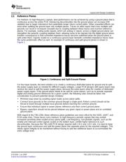
1 Continuous and Split Ground Planes ............................................................ 3
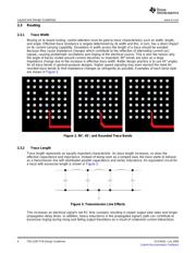
2 90 ° , 45 ° , and Rounded Trace Bends ............................................................ 4
3 Transmission Line Effects ......................................................................... 4
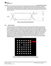
4 Power and Ground Rail Bounce .................................................................. 5
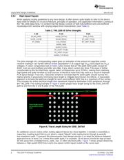
5 Leadaway Trace Routing for BGA or WCSP Packages ....................................... 5
6 Trace Length Sizing for SDIO_DATA0 .......................................................... 6
7 Proper High-Speed Trace Routing for Crosstalk Reduction .................................. 7
8 Cross-Sectional View of Blind, Buried, and Traditional Vias .................................. 8
9 250- µ m and 150- µ m Via Sizing for TWL1200 and WL1271/3 Pads ......................... 8
10 Proper TWL1200 Power Supply Decoupling .................................................... 9
11 TWL1200 Reference Design .................................................................... 10
List of Tables
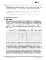
1 Four-Layer Stackup for TWL1200 PCB Design ................................................ 2
2 TWL1200 I/O Drive Strengths..................................................................... 6
SCEA042 – July 2009 TWL1200 PCB Design Guidelines 1
Submit Documentation Feedback
Verzeichnis