
herunterladen
1 PCB Layout Guidelines
Application Report
SLEA073A – July 2009 – Revised August 2009
TVP5158 PCB Layout Guidelines
.....................................................................................................................................................
• Ensure that power bus/plane routing is adequate to handle current requirements of device.
– 1.1VD and 1.8VA are the highest current supplies.
• The typical current for 1.8VA is approximately 170 mA.
• The typical current for 1.1VD is approximately 156 mA.
– The typical current of 3.3VD is approximately 40 mA.
– The typical current of 1.1VA is approximately 20 mA.
– The typical current of 3.3VA is approximately 5 mA.
Note: Typical current numbers are based on 4-CH D1 mode at 108 MHz .
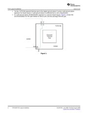
• Place TVP5158 as close as possible to the video/audio input jack.
• All device decoupling capacitors should be placed near the power and GND pins of the device.
• Keep reasonable clearances between the 27-MHz crystal/associated circuitry and adjacent audio/video
trace routing. Reasonable clearances of eight to ten times the associated trace width, ground shields
placed around audio/video traces, and placing a cutout in the ground plane and ground fill layers
around the 27-MHz crystal and associated circuitry all help isolate the crystal input.
• XTAL_REF input, pin 100, should be connected directly to crystal load capacitors. A 0- Ω resistor to
analog ground, VSSA, should be added to XTAL_REF input/crystal load capacitor junction to provide
flexibility to the crystal reference connection.
• All audio and video input traces should have a minimum clearance of ten times the trace width
between each other and other adjacent traces to minimize potential crosstalk between inputs.
• VIN_x_P and VIN_x_N should be routed side by side as differential lines. The clearance between two
traces should two to three times the trace width.
• Maintain a CVBS video input trace impedance of 75 Ω .
• Maintain reasonable routing clearance (six to eight times trace width) between the digital video
bus/clock and the digital audio bus routing.
• SDA/SCL traces should be routed together and have a minimum clearance of ten times the trace width
from any adjacent traces.
• Digital video output traces, including clocks to the input of DSP and other backend processors, should
be line-length matched. This is particularly important when the maximum data rate of 108 MHz is used.
• Digital video output traces, including the clock, should be less than six inches long between TVP5158
and backend processors, such as TI DaVinci™ HD.
– Maximum specified loading is 10 pF for data rates equal to or lower than 81 MHz.
– Maximum specified loading is 6 pF for data rates of 108 MHz.
– Minimize vias in digital video/clock bus routing between TVP5158 and backend processors.
– 10- Ω to 22- Ω series termination in the clock line is recommended.
• Digital video output traces should be line-length matched. (The maximum data rate of cascade input is
54 MHz.)
• All high-speed signals routed on the bottom of the board should be routed over solid power/ground
planes and not routed over power/ground splits. Route signals over their associated power/ground
plane where possible.
• Use ground fills on the top and bottom of the board for additional signal isolation.
SLEA073A – July 2009 – Revised August 2009 TVP5158 PCB Layout Guidelines 1
Submit Documentation Feedback