
herunterladen
1 Introduction
1.1 Description
1.2 TPA2013D1EVM Specifications
User's Guide
SLOU194 – August 2007
TPA2013D1EVM
Contents
1 Introduction ................................................................................................................... 1
2 Operation ..................................................................................................................... 2
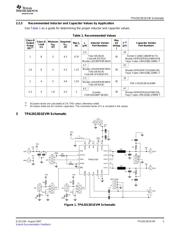
3 TPA2013D1EVM Schematic ............................................................................................... 5
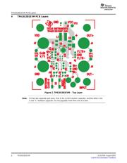
4 TPA2013D1EVM PCB Layers ............................................................................................. 6
5 TPA2013D1EVM Parts List ................................................................................................. 8
List of Figures
1 TPA2013D1EVM Schematic ............................................................................................... 5
2 TPA2013D1EVM – Top Layer ............................................................................................. 6
3 TPA2013D1EVM – Bottom Layer.......................................................................................... 7
List of Tables
1 Recommended Values ...................................................................................................... 5
2 TPA2013D1EVM Parts List ................................................................................................. 8
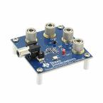
This section provides an overview of the Texas Instruments (TI) TPA2013D1 audio amplifier evaluation
module (TPA2013D1EVM). It includes a brief description of the module and a list of EVM specifications.
The TPA2013D1 is a 2.7-W Class-D amplifier with built-in boost converter. It drives up to 2.7 W (10% THD
+ N) into a 4- Ω speaker from low supply voltages.
The TPA2013D1 audio power amplifier evaluation module is a complete, stand-alone audio board. It
contains the TPA2013D1 QFN (RGP) Class-D audio power amplifier with an integrated boost converter.
All components and the evaluation module are Pb-Free.
V
DD
Supply voltage range –0.3 V to 5.5 V
I
DD
Supply current 2 A Maximum
P
O
Continuous output power per channel, 4 Ω , V
DD
= 3.6 V, V
CC
= 5.5 V 2.7 W
V
I
Audio Input Voltage -0.3 V to V
DD
+ 0.3 V
R
L
Minimum load impedance 4 Ω
SLOU194 – August 2007 TPA2013D1EVM 1
Submit Documentation Feedback
Verzeichnis
- ・ Blockdiagramm on Seite 5
- ・ Anwendungsbereich on Seite 10
- ・ Teilenummernliste on Seite 5