
herunterladen
TMS320DM8148, TMS320DM8147, TMS320DM8146
www.ti.com
SPRS647D –MARCH 2011–REVISED SEPTEMBER 2012
TMS320DM814x DaVinci™
Video Processors
Check for Samples: TMS320DM8148, TMS320DM8147, TMS320DM8146
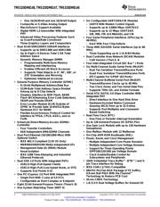
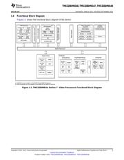
1 High-Performance System-on-Chip (SoC)
1.1 Features
12
– 32K-Byte L1D RAM/Cache
• High-Performance DaVinci™ Video Processors
– 256K-Byte L2 Unified Mapped RAM/Caches
– Up to 1-GHz ARM® Cortex™-A8 RISC Core
With ECC
– Up to 750-MHz C674x™ VLIW DSP
• DSP/EDMA Memory Management Unit
– Up to 6000/4500 C674x™ MIPS/MFLOPS
(DEMMU)
– Fully Software-Compatible with C67x+™,
– Maps C674x DSP and EDMA TC Memory
C64x+™
Accesses to System Addresses
• ARM® Cortex™-A8 Core
• 128K-Bytes On-Chip Memory Controller
– ARMv7 Architecture
(OCMC) RAM
• In-Order, Dual-Issue, Superscalar
• Imaging Subsystem (ISS)
Processor Core
– Camera Sensor Connection
• NEON™ Multimedia Architecture
• Parallel Connection for Raw (up to 16-Bit)
• Supports Integer and Floating Point
and BT.656/BT.1120 (8-/16-bit)
• Jazelle® RCT Execution Environment
– Image Sensor Interface (ISIF) for Handling
• ARM® Cortex™-A8 Memory Architecture
Image/Video Data From the Camera Sensor
– 32K-Byte Instruction and Data Caches
– Resizer
– 512K-Byte L2 Cache
• Resizing Image/Video From 1/16x to 8x
– 64K-Byte RAM, 48K-Byte Boot ROM
• Generating Two Different Resizing
• TMS320C674x™ Floating-Point VLIW DSP
Outputs Concurrently
– 64 General-Purpose Registers (32-Bit)
• Programmable High-Definition Video Image
– Six ALU (32-/40-Bit) Functional Units
Coprocessing (HDVICP v2) Engine
• Supports 32-Bit Integer, SP (IEEE Single
– Encode, Decode, Transcode Operations
Precision/32-Bit) and DP (IEEE Double
– H.264, MPEG2, VC1, MPEG4, SP/ASP,
Precision/64-Bit) Floating Point
JPEG/MJPEG
• Supports up to Four SP Adds Per Clock
• Media Controller
and Four DP Adds Every Two Clocks
– Controls the HDVPSS, HDVICP2, and ISS
• Supports up to Two Floating-Point (SP or
• SGX530 3D Graphics Engine
DP) Approximate Reciprocal or Square
– Delivers up to 25 MPoly/sec
Root Operations Per Cycle
– Universal Scalable Shader Engine
– Two Multiply Functional Units
– Direct3D Mobile, OpenGLES 1.1 and 2.0,
• Mixed-Precision IEEE Floating-Point
OpenVG 1.0, OpenMax API Support
Multiply Supported up to:
– Advanced Geometry DMA Driven Operation
– 2 SP x SP → SP Per Clock
– Programmable HQ Image Anti-Aliasing
– 2 SP x SP → DP Every Two Clocks
• Endianness
– 2 SP x DP → DP Every Three Clocks
– ARM/DSP Instructions/Data – Little Endian
– 2 DP x DP → DP Every Four Clocks
• HD Video Processing Subsystem (HDVPSS)
• Fixed-Point Multiply Supports Two 32 x
– Two 165 MHz HD Video Capture Inputs
32 Multiplies, Four 16 x 16-bit Multiplies
• One 16/24-bit Input, Splittable into Dual 8-
including Complex Multiplies, or Eight 8 x
bit SD Capture Ports
8-Bit Multiplies per Clock Cycle
• One 8/16/24-bit Input
• C674x™ Two-Level Memory Architecture
• One 8-bit Only Input
– 32K-Byte L1P RAM/Cache With EDC
– Two 165 MHz HD Video Display Outputs
1
Please be aware that an important notice concerning availability, standard warranty, and use in critical applications of
Texas Instruments semiconductor products and disclaimers thereto appears at the end of this data sheet.
2All trademarks are the property of their respective owners.
PRODUCTION DATA information is current as of publication date. Products conform to
Copyright © 2011–2012, Texas Instruments Incorporated
specifications per the terms of the Texas Instruments standard warranty. Production
processing does not necessarily include testing of all parameters.
Verzeichnis
- ・ Konfiguration des Pinbelegungsdiagramms on Seite 153 Seite 154
- ・ Abmessungen des Paketumrisses on Seite 367
- ・ Blockdiagramm on Seite 5 Seite 15 Seite 22 Seite 206 Seite 265
- ・ Typisches Anwendungsschaltbild on Seite 345
- ・ Technische Daten on Seite 175 Seite 201 Seite 265 Seite 266 Seite 267
- ・ Anwendungsbereich on Seite 3 Seite 370
- ・ Elektrische Spezifikation on Seite 169 Seite 179 Seite 180