

herunterladen
V
ref
Input
V
KA
I
KA
Copyright © 2016, Texas Instruments Incorporated
Product
Folder
Sample &
Buy
Technical
Documents
Tools &
Software
Support &
Community
Reference
Design
An IMPORTANT NOTICE at the end of this data sheet addresses availability, warranty, changes, use in safety-critical applications,
intellectual property matters and other important disclaimers. PRODUCTION DATA.
TL1431
,
TL1431M
SLVS062N –DECEMBER 1991–REVISED OCTOBER 2016
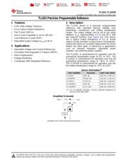
TL1431 Precision Programmable Reference
1
1 Features
1
• 0.4% Initial Voltage Tolerance
• 0.2-Ω Typical Output Impedance
• Fast Turnon (500 ns)
• Sink Current Capability (1 mA to 100 mA)
• Low Reference Current (REF)
• Adjustable Output Voltage (V
I(ref)
to 36 V)
2 Applications
• Adjustable Voltage and Current Referencing
• Secondary Side Regulation in Flyback SMPSs
• Zener Replacement
• Voltage Monitoring
• Comparator With Integrated Reference
3 Description
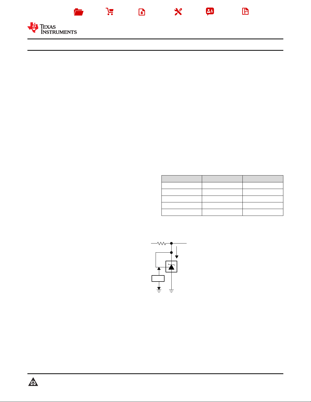
The TL1431 device is a precision programmable
reference with specified thermal stability over
automotive, commercial, and military temperature
ranges. The output voltage can be set to any value
between V
I(ref)
(approximately 2.5 V) and 36 V with
two external resistors (see Figure 25). This device
has a typical output impedance of 0.2 Ω. Active
output circuitry provides a sharp turnon characteristic,
making the device an excellent replacement for Zener
diodes and other types of references in applications
such as onboard regulation, adjustable power
supplies, and switching power supplies.
The TL1431C is characterized for operation over the
commercial temperature range of 0°C to 70°C. The
TL1431Q is characterized for operation over the full
automotive temperature range of –40°C to 125°C.
The TL1431M is characterized for operation over the
full military temperature range of –55°C to 125°C.
Device Information
(1)
PART NUMBER PACKAGE BODY SIZE (NOM)
TL1431D SOIC (8) 3.90 mm × 4.90 mm
TL1431PW TSSOP (8) 4.40 mm × 3.00 mm
TL1431LP TO-92 (3) 4.83 mm × 3.68 mm
TL1431MJG CDIP (8) 9.58 mm x 6.67 mm
TL1431MFK LCCC (20) 8.89 mm x 8.89 mm
(1) For all available packages, see the orderable addendum at
the end of the data sheet.
Simplified Schematic
Verzeichnis
- ・ Konfiguration des Pinbelegungsdiagramms on Seite 3
- ・ Abmessungen des Paketumrisses on Seite 22 Seite 23 Seite 26 Seite 27 Seite 34
- ・ Paket-Footprint-Pad-Layout on Seite 35
- ・ Markierungsinformationen on Seite 22 Seite 23 Seite 24
- ・ Blockdiagramm on Seite 1 Seite 12 Seite 13 Seite 15
- ・ Typisches Anwendungsschaltbild on Seite 15
- ・ Technische Daten on Seite 4
- ・ Anwendungsbereich on Seite 1 Seite 24 Seite 25 Seite 38
- ・ Elektrische Spezifikation on Seite 5 Seite 6 Seite 7 Seite 13 Seite 16