
herunterladen
User's Guide
SNVA413C–October 2009–Revised May 2013
AN-2000 LM5060EVAL Evaluation Board
1 Introduction
The LM5060 evaluation board is designed to demonstrate the capabilities of the LM5060 high side
protection controller with low quiescent current. It is intended for evaluation of the functions of the
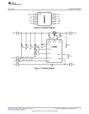
LM5060. One high side N-channel power MOSFET is used. The LM5060 evaluation board schematic is
shown in Figure 7. The evaluation board is designed to highlight applications with a small solution size.
For more information about LM5060 functional and electrical characteristics, see the LM5060 High-Side
Protection Controller With Low Quiescent Current Data Sheet (SNVS628).
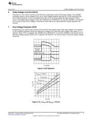
2 Operating Range
• Maximum Input Voltage, OVP: 37 V
• Minimum Input Voltage, UVLO: 9 V
• Output Current Range: 0A to 5.0A
• Ambient Temperature Range 0°C to 50°C
• Board Size 1.35in x 2.25in
To aid in the design and evaluation of high-side protection controller solutions based on the LM5060, the
evaluation board can be re-configured for different input voltage ranges by modifying the under-voltage
lock-out (UVLO) and the over-voltage protection (OVP) resistive divider (R1, R2, and R3) as well as the
protection transient voltage suppressor diode D1.
The load current capability may be increased above 5A of by changing the value of resistor R4. The PCB
layout has not been tested for currents above 5A, so this should only be done with some degree of
caution.
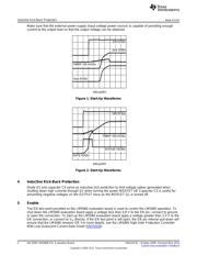
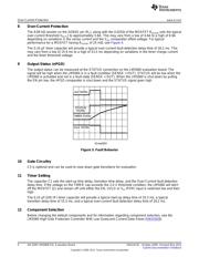
Typical evaluation board performance and characteristics curves are shown in Figure 1 through Figure 5.
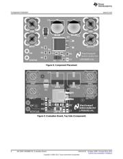
The PCB layout is shown in Figure 9 and Figure 10. Test points are provided to enable easy connection
and monitoring of critical signals.
3 Evaluation Board Start-Up
Before applying power to the LM5060 evaluation board, all external connections should be verified. The
external power supply must be turned off and connected with proper polarity to the INPUT and GND
posts. A load resistor should be connected between the OUTPUT and GND posts as desired. A resistive
load keeps the current through Q1 during turn-on relatively low. Electronic load equipment tends to be
very low impedance during voltage rise so that the transistor Q1 will see very high currents during turn-on
when using such loads. Though resistive loads are suggested for use with the LM5060 evaluation board,
electronic loads can be used with caution as well. The output voltage can be monitored with a multi-meter
or oscilloscope at the OUTPUT post.
Once all connections to the evaluation board have been verified, input power can be applied. A load
resistor or electronic load does not require connection during startup. If the EN test point is pulled high
(see the threshold voltage in the Electrical Characteristics section of the LM5060 High-Side Protection
Controller With Low Quiescent Current Data Sheet (SNVS628)), the output voltage will ramp up when an
input voltage is applied.
For the evaluation board to start up, the EN pin needs to be pulled high. A lab cable is required from the
EN pin to the V
IN
pin or other voltage source higher than 2.0 V.
All trademarks are the property of their respective owners.
1
SNVA413C–October 2009–Revised May 2013 AN-2000 LM5060EVAL Evaluation Board
Submit Documentation Feedback
Copyright © 2009–2013, Texas Instruments Incorporated
Verzeichnis
- ・ Blockdiagramm on Seite 5
- ・ Anwendungsbereich on Seite 8
- ・ Elektrische Spezifikation on Seite 1