

herunterladen
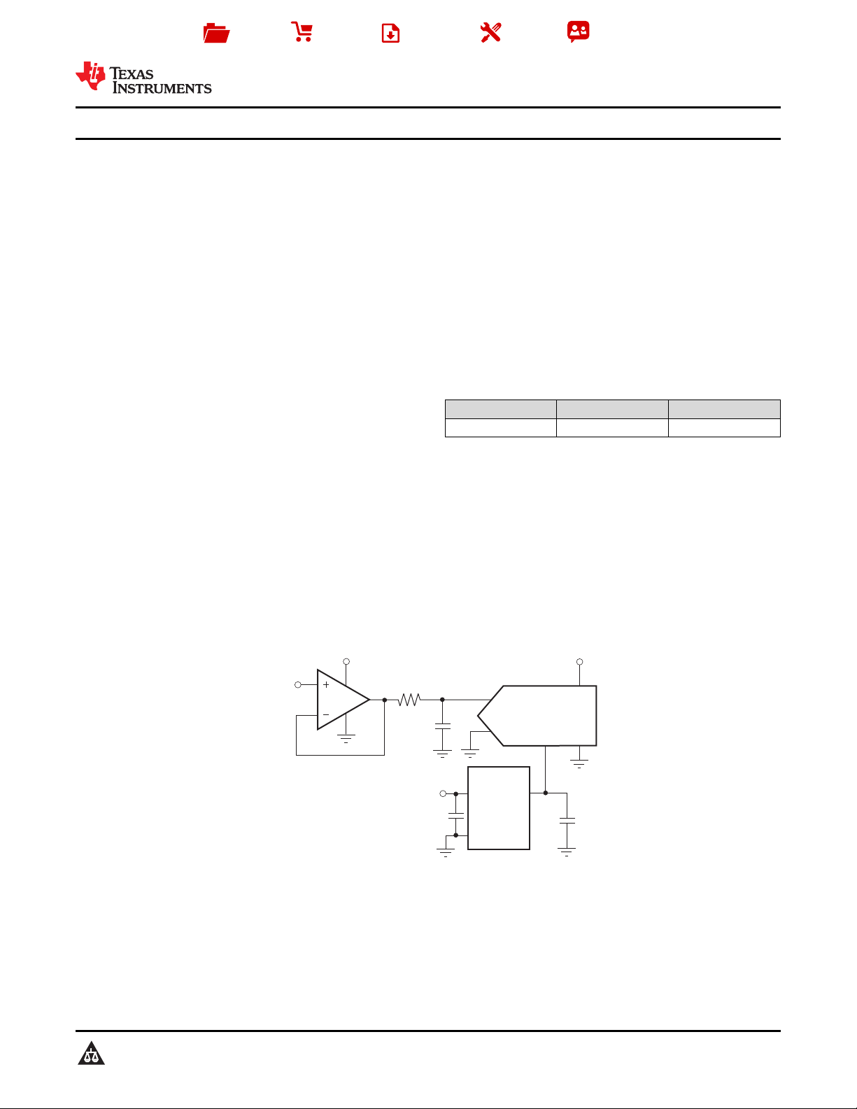
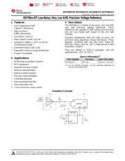
ADS8326
REF5040
REF
V
OUT
GND
+IN
- IN
V
IN
+5 V
OPA365
Input
Signal
0 V to 4 V
+5 V +5 V
V
DD
GND
C
BYPASS
1 µF
R
1
50 Ω
C
1
1.2 nF
C
2
22 µf
Product
Folder
Sample &
Buy
Technical
Documents
Tools &
Software
Support &
Community
REF5020-EP
,
REF5025-EP
,
REF5040-EP
,
REF5050-EP
SBOS471B –APRIL 2010–REVISED JUNE 2015
REF50xx-EP Low-Noise, Very Low Drift, Precision Voltage Reference
1 Features 3 Description
The REF50xx is a family of low-noise, very low-drift,
1
• Low Temperature Drift:
very high precision voltage references. These
5 ppm/°C (Maximum)
references are capable of both sinking and sourcing,
• High Accuracy:
and are very robust with regard to line and load
0.08% (Maximum)
changes.
• Low Noise: 3 μV
PP
/V
Excellent temperature drift and high accuracy are
• High Output Current: ±10 mA
achieved using proprietary design techniques. These
features, combined with very low noise, make the
• Available in Military (–55°C to 125°C)
REF50xx family ideal for use in high-precision data
Temperature Range
(1)
acquisition systems.
• Extended Product Life Cycle
They are offered in SOIC-8 packages, and are
• Extended Product-Change Notification
specified from –55°C to 125°C.
• Product Traceability
Device Information
(1)
2 Applications
PART NUMBER PACKAGE BODY SIZE (NOM)
• 16-Bit Data Acquisition Systems
REF50xx-EP SOIC (8) 4.90 mm × 3.91 mm
• ATE Equipment
(1) For all available packages, see the orderable addendum at
the end of the data sheet.
• Industrial Process Control
• Medical Instrumentation
• Optical Control Systems
• Precision Instrumentation
• Controlled Baseline
• One Assembly/Test Site
• One Fabrication Site
(1) Custom temperature ranges available
Simplified Schematic
1
An IMPORTANT NOTICE at the end of this data sheet addresses availability, warranty, changes, use in safety-critical applications,
intellectual property matters and other important disclaimers. PRODUCTION DATA.
Verzeichnis
- ・ Konfiguration des Pinbelegungsdiagramms on Seite 3
- ・ Abmessungen des Paketumrisses on Seite 23 Seite 25 Seite 26
- ・ Markierungsinformationen on Seite 23 Seite 24
- ・ Blockdiagramm on Seite 1 Seite 10 Seite 11 Seite 13
- ・ Typisches Anwendungsschaltbild on Seite 13 Seite 14 Seite 15 Seite 16
- ・ Technische Daten on Seite 3
- ・ Anwendungsbereich on Seite 1 Seite 11 Seite 13 Seite 14 Seite 15
- ・ Elektrische Spezifikation on Seite 4 Seite 5 Seite 11