
herunterladen
Product
Folder
Sample &
Buy
Technical
Documents
Tools &
Software
Support &
Community
OMAP-L138
www.ti.com
SPRS586F –JUNE 2009–REVISED AUGUST 2013
OMAP-L138 C6000™ DSP+ARM® Processor
Check for Samples: OMAP-L138
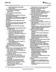
1 OMAP-L138 C6000™ DSP+ARM Processor
1.1 Features
12
Precision/32-Bit) and DP (IEEE Double
• Dual-Core SoC
Precision/64-Bit) Floating Point
– 375-/456-MHz ARM926EJ-S™ RISC MPU
• Supports up to Four SP Additions Per
– 375-/456-MHz C674x Fixed- and Floating-
Clock, Four DP Additions Every Two
Point VLIW DSP
Clocks
• ARM926EJ-S Core
• Supports up to Two Floating-Point (SP or
– 32- and 16-Bit (Thumb®) Instructions
DP) Reciprocal Approximation (RCPxP)
– DSP Instruction Extensions
and Square-Root Reciprocal
– Single-Cycle MAC
Approximation (RSQRxP) Operations Per
– ARM Jazelle® Technology
Cycle
– EmbeddedICE-RT™ for Real-Time Debug
– Two Multiply Functional Units:
• ARM9™ Memory Architecture
• Mixed-Precision IEEE Floating-Point
Multiply Supported up to:
– 16KB of Instruction Cache
– 2 SP x SP → SP Per Clock
– 16KB of Data Cache
– 2 SP x SP → DP Every Two Clocks
– 8KB of RAM (Vector Table)
– 2 SP x DP → DP Every Three Clocks
– 64KB of ROM
– 2 DP x DP → DP Every Four Clocks
• C674x Instruction Set Features
• Fixed-Point Multiply Supports Two 32 x
– Superset of the C67x+™ and C64x+™ ISAs
32-Bit Multiplies, Four 16 x 16-Bit
– Up to 3648 MIPS and 2746 MFLOPS
Multiplies, or Eight 8 x 8-Bit Multiplies per
– Byte-Addressable (8-, 16-, 32-, and 64-Bit
Clock Cycle, and Complex Multiples
Data)
– Instruction Packing Reduces Code Size
– 8-Bit Overflow Protection
– All Instructions Conditional
– Bit-Field Extract, Set, Clear
– Hardware Support for Modulo Loop
– Normalization, Saturation, Bit-Counting
Operation
– Compact 16-Bit Instructions
– Protected Mode Operation
• C674x Two-Level Cache Memory Architecture
– Exceptions Support for Error Detection and
– 32KB of L1P Program RAM/Cache
Program Redirection
– 32KB of L1D Data RAM/Cache
• Software Support
– 256KB of L2 Unified Mapped RAM/Cache
– TI DSP/BIOS™
– Flexible RAM/Cache Partition (L1 and L2)
– Chip Support Library and DSP Library
• Enhanced Direct-Memory-Access Controller 3
• 128KB of RAM Shared Memory
(EDMA3):
• 1.8-V or 3.3-V LVCMOS I/Os (Except for USB
– 2 Channel Controllers
and DDR2 Interfaces)
– 3 Transfer Controllers
• Two External Memory Interfaces:
– 64 Independent DMA Channels
– EMIFA
– 16 Quick DMA Channels
• NOR (8- or 16-Bit-Wide Data)
– Programmable Transfer Burst Size
• NAND (8- or 16-Bit-Wide Data)
• TMS320C674x™ Floating-Point VLIW DSP Core
• 16-Bit SDRAM with 128-MB Address
– Load-Store Architecture with Nonaligned
Space
Support
– DDR2/Mobile DDR Memory Controller with
– 64 General-Purpose Registers (32 Bit)
one of the following:
– Six ALU (32- and 40-Bit) Functional Units
• 16-Bit DDR2 SDRAM with 256-MB
• Supports 32-Bit Integer, SP (IEEE Single
Address Space
1
Please be aware that an important notice concerning availability, standard warranty, and use in critical applications of
Texas Instruments semiconductor products and disclaimers thereto appears at the end of this data sheet.
2All trademarks are the property of their respective owners.
PRODUCTION DATA information is current as of publication date. Products conform to
Copyright © 2009–2013, Texas Instruments Incorporated
specifications per the terms of the Texas Instruments standard warranty. Production
processing does not necessarily include testing of all parameters.
Verzeichnis
- ・ Konfiguration des Pinbelegungsdiagramms on Seite 27 Seite 72
- ・ Abmessungen des Paketumrisses on Seite 282 Seite 283
- ・ Markierungsinformationen on Seite 282 Seite 283
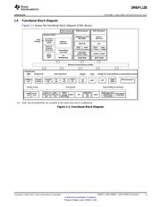
- ・ Blockdiagramm on Seite 5 Seite 14 Seite 129 Seite 130 Seite 131
- ・ Technische Daten on Seite 78 Seite 83 Seite 84 Seite 85 Seite 86
- ・ Anwendungsbereich on Seite 3 Seite 287
- ・ Elektrische Spezifikation on Seite 82 Seite 83 Seite 84 Seite 85 Seite 86