

herunterladen
© Semiconductor Components Industries, LLC, 2015
January, 2015 − Rev. 2
1 Publication Order Number:
AND8195/D
AND8195/D
Board Mounting Notes for
SO8-Flat Lead
Introduction
Various ON Semiconductor devices are packaged in an
advanced power leadless package named Quad Flat
No-Lead (QFN) Package. The power QFN platform
represents the latest in surface mount packaging technology.
It is important that the design of the Printed Circuit Board
(PCB) and the assembly process follow the suggested
guidelines outlined in this document.
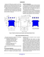
SO8FL PACKAGE OVERVIEW
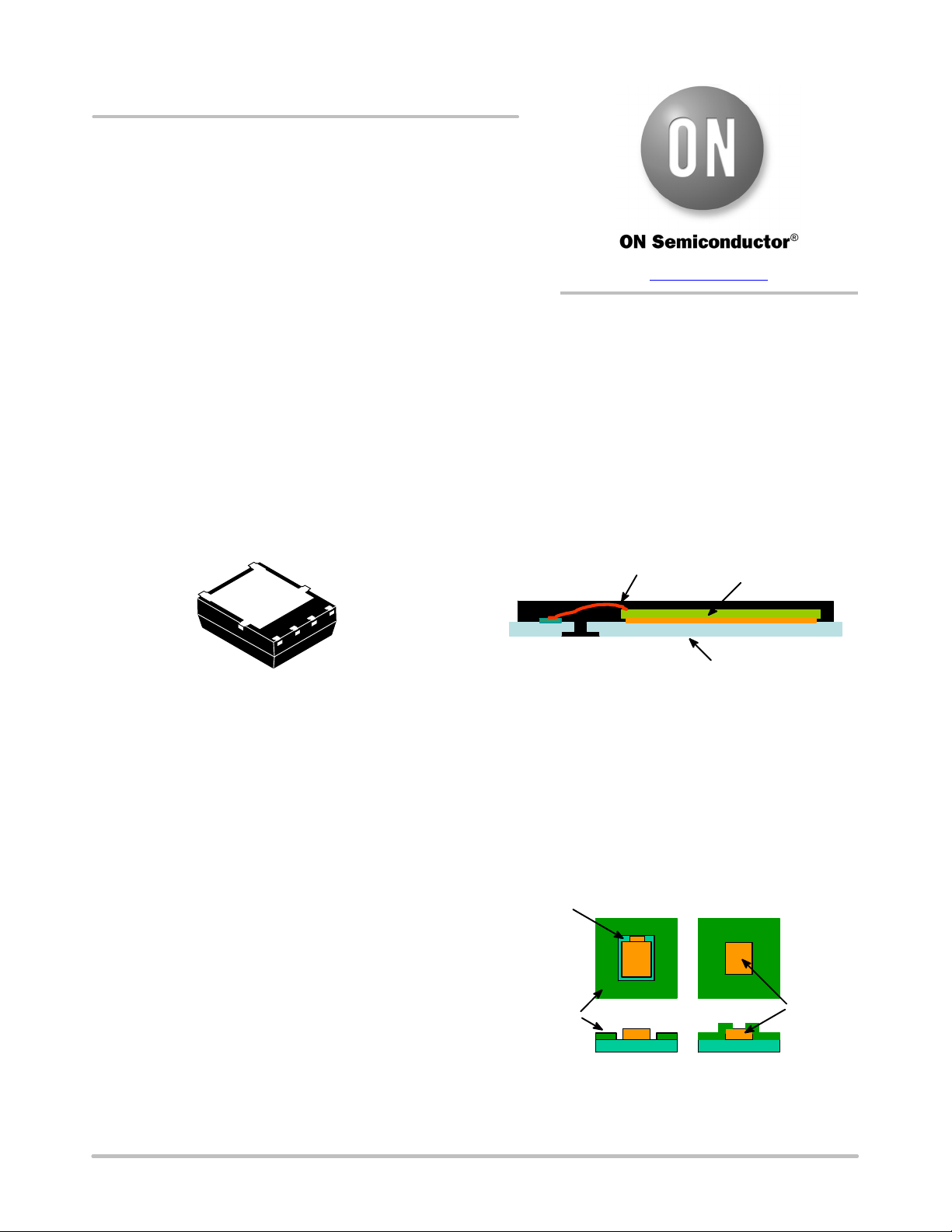
The SO8FL package was created to allow a larger
MOSFET die to fit into a standard SO8IC footprint. This
package uses a lead frame design that allows the leads to
stick out beyond the molded body size. This feature allows
the customer to see the solder fillet during visual inspection.
See Figure 1 below.
Figure 1. The Underside of an SO8FL Package
Figure 2 illustrates how the package height is reduced to
a minimum by having both die and wire bond pads on the
same plane. When mounted, the leads and the body are
directly attached to the board without a space-consuming
standoff which is inherent in a leaded package.
Figure 2 also illustrates how the ends of the leads go past
the edge of the molded package. This configuration allows
for the maximum die size within a given footprint, which in
turn maximize the board space utilization.
Figure 2. Cross-section of SO8FL Package
Wire Bond
Die
Lead Frame
In addition to these features, the SO8FL package has
excellent thermal dissipation and reduced electrical
parasitic elements due to its efficient and compact design.
PRINTED CIRCUIT BOARD DESIGN CONSIDERATIONS
SMD and NSMD Pad Configurations
There are two different types of PCB pad configurations
commonly used for surface mount QFN style packages.
These different I/O configurations are:
• Non Solder Masked Defined (NSMD)
• Solder Masked Defined (SMD)
As their titles describe, the NSMD contact pads have the
solder mask pulled away from the solderable metallization,
while the SMD pads have the solder mask over the edge of
the metallization, as shown in Figure 3. With the SMD pads,
the solder mask restricts the flow of solder paste to the top
of the metallization preventing the solder from flowing
along the sides of the metal pad. This is different from the
NSMD configuration where the solder will flow around both
the top and the sides of the metallization.
Figure 3. Comparison of NSMD vs. SMD Pads
NSMD SMD
Solder Mask
Opening
Solderable
Pad
Solder Mask
Overlay
APPLICATION NOTE
www.onsemi.com
Verzeichnis