
herunterladen
Semiconductor Components Industries, LLC, 2013
May, 2013 − Rev. 3
1 Publication Order Number:
NCP612/D
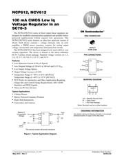
NCP612, NCV612
100 mA CMOS Low Iq
Voltage Regulator in an
SC70-5
The NCP612/NCV612 series of fixed output linear regulators are
designed for handheld communication equipment and portable battery
powered applications which require low quiescent. The
NCP612/NCV612 series features an ultra−low quiescent current of
40 A. Each device contains a voltage reference unit, an error
amplifier, a PMOS power transistor, resistors for setting output
voltage, current limit, and temperature limit protection circuits.
The NCP612/NCV612 has been designed to be used with low cost
ceramic capacitors. The device is housed in the micro−miniature
SC70−5 surface mount package. Standard voltage versions are 1.5,
1.8, 2.5, 2.7, 2.8, 3.0, 3.1, 3.3, 3.7, and 5.0 V.
Features
Low Quiescent Current of 40 A Typical
Low Dropout Voltage of 230 mV at 100 mA and 3.0 V V
out
Low Output Voltage Option
Output Voltage Accuracy of 2.0%
Temperature Range of −40C to 85C (NCP612)
Temperature Range of −40C to 125C (NCV612)
NCV Prefix for Automotive and Other Applications Requiring
Unique Site and Control Change Requirements; AEC−Q100
Qualified and PPAP Capable
These are Pb−Free Devices
Typical Applications
Cellular Phones
Battery Powered Consumer Products
Hand−Held Instruments
Camcorders and Cameras
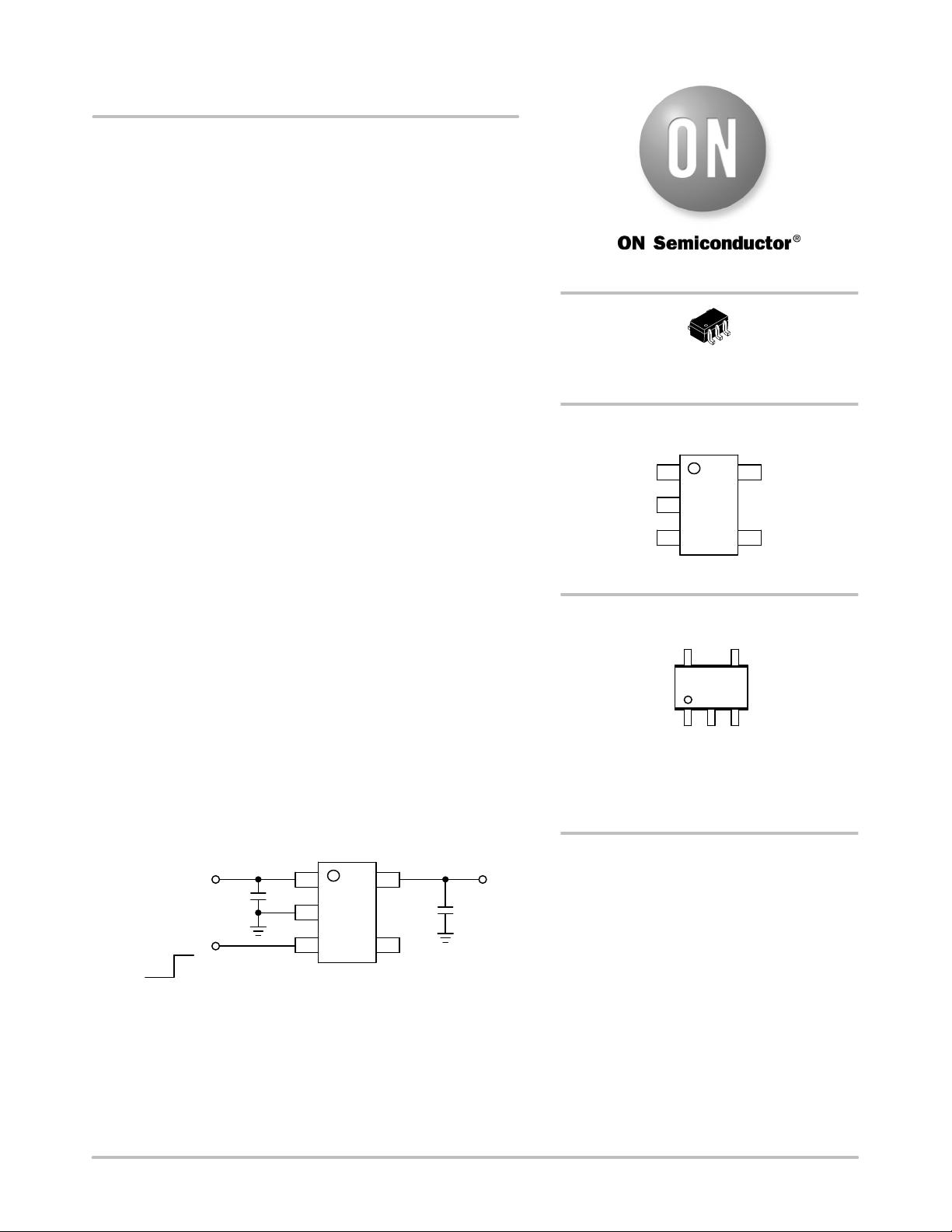
Figure 1. Typical Application Diagram
This device contains 86 active transistors
Vout
Battery or
Unregulated
Voltage
C1
C2
OFF
ON
1
2
3
5
4
+
+
See detailed ordering and shipping information in the package
dimensions section on page 8 of this data sheet.
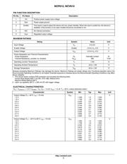
ORDERING INFORMATION
SC70−5
CASE 419A
PIN CONNECTIONS
1
3
N/C
V
in
2
Gnd
Enable
4
V
out
5
(Top View)
xxx = Specific Device Code
M = Date Code*
G = Pb−Free Package
MARKING DIAGRAM
http://onsemi.com
1
5
xxxM G
G
(Note: Microdot may be in either location)
Verzeichnis
- ・ Konfiguration des Pinbelegungsdiagramms on Seite 1
- ・ Abmessungen des Paketumrisses on Seite 9
- ・ Teilenummerierungssystem on Seite 1 Seite 8 Seite 9
- ・ Markierungsinformationen on Seite 1 Seite 8 Seite 9
- ・ Typisches Anwendungsschaltbild on Seite 1
- ・ Beschreibung der Funktionen on Seite 2
- ・ Anwendungsbereich on Seite 1 Seite 7 Seite 8
- ・ Elektrische Spezifikation on Seite 2 Seite 3