
herunterladen
Semiconductor Components Industries, LLC, 2013
May, 2013 − Rev. 20
1 Publication Order Number:
NCP502/D
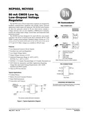
NCP502, NCV502
80 mA CMOS Low Iq,
Low-Dropout Voltage
Regulator
The NCP502 series of fixed output linear regulators are designed for
handheld communication equipment and portable battery powered
applications which require low quiescent. The NCP502 series features
an ultra−low quiescent current of 40 A. Each device contains a
voltage reference unit, an error amplifier, a PMOS power transistor,
resistors for setting output voltage, current limit, and temperature limit
protection circuits.
The NCP502 has been designed to be used with low cost ceramic
capacitors. The device is housed in the micro−miniature SC70−5 and
TSOP−5 surface mount packages. Standard voltage versions are 1.5 V,
1.8 V, 2.5 V, 2.7 V, 2.8 V, 2.9 V, 3.0 V, 3.1 V, 3.3 V, 3.4 V, 3.5 V, 3.6 V,
3.7 V and 5.0 V. Other voltages are available in 100 mV steps.
Features
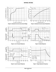
Low Quiescent Current of 40 A Typical
Excellent Line and Load Regulation
Low Output Voltage Option
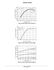
Output Voltage Accuracy of 2.0%
Industrial Temperature Range of −40C to 85C,
NCV502, T
A
= −40C to 125C
NCP502: 1.3 V Enable Threshold High, 0.3 V Enable Threshold Low
NCV Prefix for Automotive and Other Applications Requiring
Unique Site and Control Change Requirements; AEC−Q100
Qualified and PPAP Capable
These are Pb−Free Devices
Typical Applications
Cellular Phones
Battery Powered Consumer Products
Hand−Held Instruments
Camcorders and Cameras
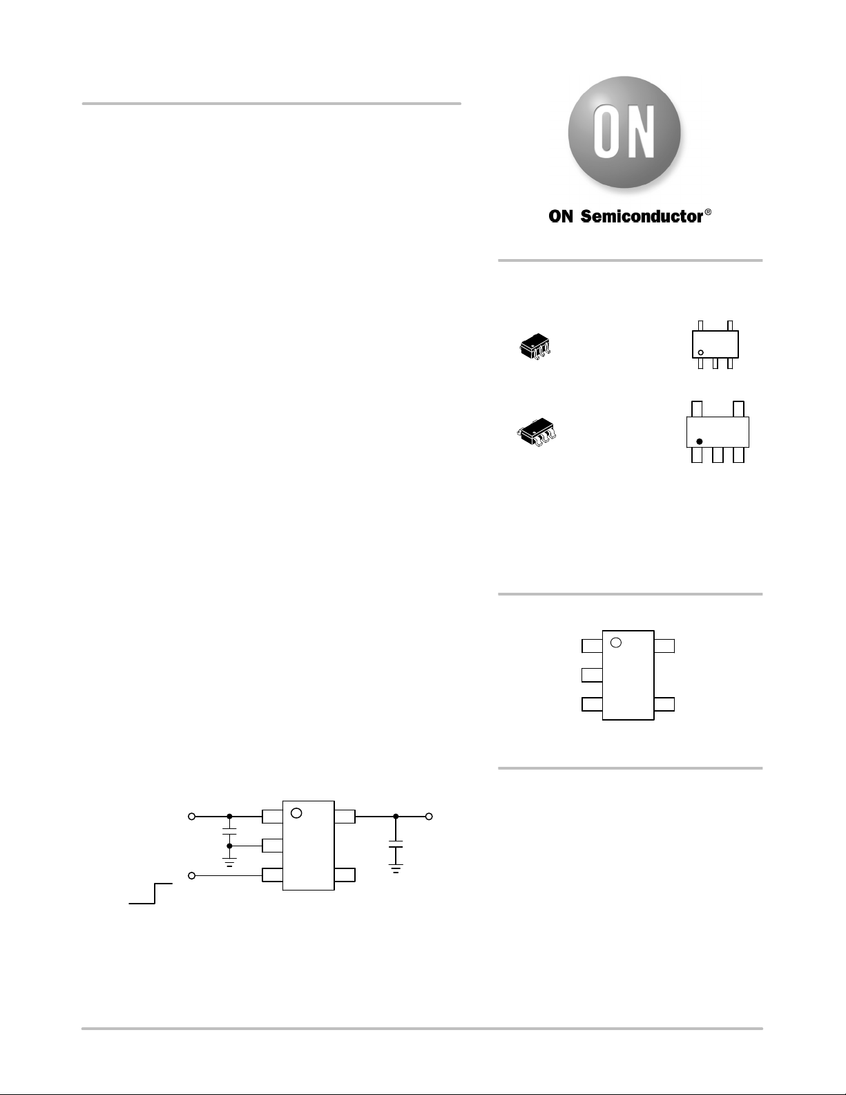
Figure 1. Typical Application Diagram
This device contains 86 active transistors
Vout
Battery or
Unregulated
Voltage
C1
C2
OFF
ON
1
2
3
5
4
+
+
See detailed ordering and shipping information in the package
dimensions section on page 7 of this data sheet.
ORDERING INFORMATION
PIN CONNECTIONS
1
3
N/C
V
in
2GND
Enable
4
V
out
5
(Top View)
xxx = Specific Device Code
A = Assembly Location
Y = Year
W = Work Week
M = Date Code
G = Pb−Free Package
MARKING
DIAGRAM
http://onsemi.com
1
2
3
4
5
SC70−5
SQ SUFFIX
CASE 419A
1
5
xxx MG
G
http://onsemi.com
(Note: Microdot may be in either location)
1
5
TSOP−5
(SOT23−5, SC59−5)
SN SUFFIX
CASE 483
1
5
xxx AYWG
G
Verzeichnis
- ・ Konfiguration des Pinbelegungsdiagramms on Seite 1
- ・ Abmessungen des Paketumrisses on Seite 8 Seite 9
- ・ Paket-Footprint-Pad-Layout on Seite 9
- ・ Teilenummerierungssystem on Seite 1 Seite 7 Seite 9
- ・ Markierungsinformationen on Seite 1 Seite 7 Seite 9
- ・ Typisches Anwendungsschaltbild on Seite 1
- ・ Beschreibung der Funktionen on Seite 2
- ・ Technische Daten on Seite 7
- ・ Anwendungsbereich on Seite 1 Seite 6 Seite 7
- ・ Elektrische Spezifikation on Seite 3