
herunterladen
DN06060/D
September 2009, Rev. 1 www.onsemi.com 1
Design Note – DN06060/D
Detection Voltage Selection Guidelines for
Application of NCP30X Family Series
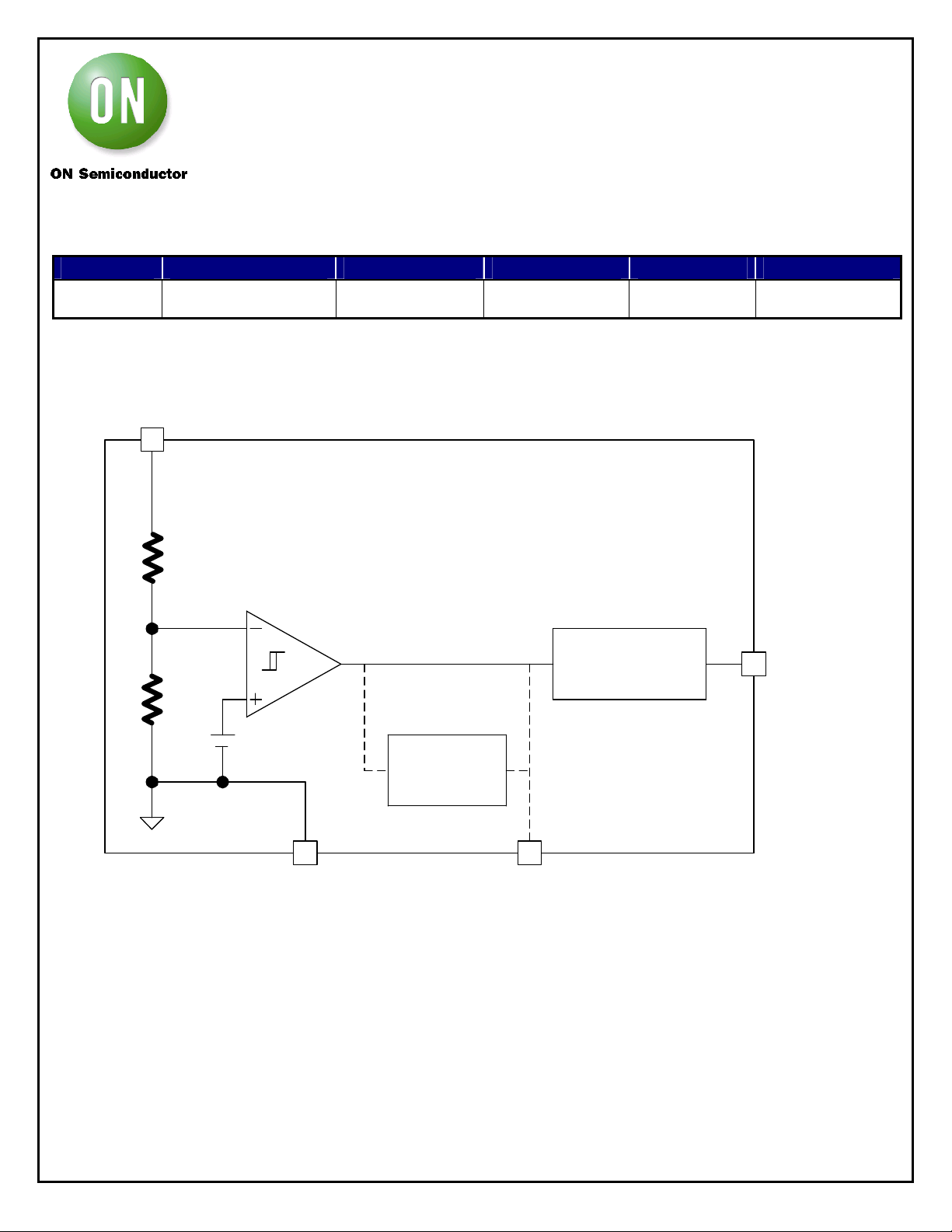
Device Application Input Voltage Output Power Topology I/O Isolation
NCP30X
Voltage Supervisory
Rest IC
N/A N/A N/A N/A
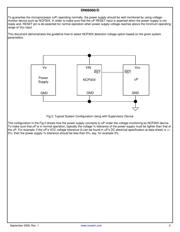
Circuit Description
VIN
CD
RESET
GND
Driver Block
for Delay
Capacitor *
Output Stage
Open Drain or
Complementary
Output
* For NCP302/303 Series
Vref
Fig 1. General block diagram of NCP30X family series
The Fig 1. shows the basic block diagram of NCP30X supervisory family series. It features a highly accurate undervoltage
detector with hysteresis. Some parts also feature an externally programmable time delay generator by adding a delay
capacitor at the CD pin. This combination of features prevents the system from erratic reset operation.