
herunterladen

© Semiconductor Components Industries, LLC, 2015
March, 2015 - Rev. 1
1 Publication Order Number:
AND9202/D
AND9202/D
A System Designer's Guide
for Building a PCIe
®
Clock
Tree while Addressing
Timing Challenges
Abstract
PCIe standard has become a popular choice for high speed
serial communication in networking, computing, industrial
and embedded systems. With increasing data rates
requirements, the reference clock performance is critical
and its specifications are more aggressive for good timing
margins in these systems. Clocking signals have to
overcome difficult system challenges for maintaining the
timing budget requirements and to provide a reliable
reference clock.
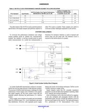
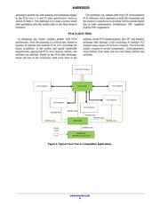
This application note focuses on the PCIe timing solutions
from ON Semiconductor catering to different clocking
architectures and various system clock trees used in the
industry. The portfolio includes crystal oscillators, clock
generators, spread spectrum (for EMI reduction) clock
generators, fanout buffers, zero delay (ZDB) buffers and
PCIe switches for Networking, Computing, Consumer and
Industrial markets. This application note also elaborates on
the best in class timing products offered by
ON Semiconductor which are suitable for systems with
stringent timing margins, thereby enabling system designers
to realize a complete clock tree with high performance
silicon solutions.
Introduction
The next generation technologies bring in the need for
faster and efficient communication with robust signal
integrity and shrinking form factors. Catering to transceiver
applications for high baud rates, many communication
protocols such as ISA, ATA, XT−IDE, PCMCIA, USB, PCI,
PCI−X, AGP, PCIe, etc. are further being developed and
adapted to meet the bandwidth demands of the next
generation technologies.
Evolution of PCIe Standard
Earlier, parallel bus model was preferred over serial
model for higher throughput. However practical speed
limitation due to clock skew, signal data skew and flight
time, and high pin count motivated the transition away from
the parallel bus model, and advanced serial communication
protocols gained prominence for their superior performance
and their compact footprint. Peripheral Component
Interconnect − Special Interest Group (PCI−SIG) introduced
a serial local computer bus protocol − Peripheral Component
Interconnect (PCI) for higher throughput, and it was later
enhanced to PCI Extended (PCI−X). Further enhancements
in the development led to PCI Express (PCIe), which is a
point−to−point full duplex serial computer expansion bus
standard developed by PCI−SIG. PCIe was designed to
replace PCI, PCI−X and AGP standards for a faster and
flexible solution.
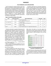
PCIe protocol has evolved over a period of time through
generations, accommodating the needs of higher speeds and
throughput – each generation of the protocol, Gen I, Gen II
and Gen III, progressively required stringent reference clock
performance. Originally intended for desktop computers,
PCIe is now a popular choice in applications like servers,
network attached storage, network switches/ routers, set top
boxes and other embedded applications for its advantages of
scalable bandwidth and flexibility. This makes the PCIe
reference clock requirements more stringent as it needs to
adhere to timing budgets of these applications while
overcoming the system challenges.
www.onsemi.com
APPLICATION NOTE
Verzeichnis