
herunterladen

Product
Folder
Sample &
Buy
Technical
Documents
Tools &
Software
Support &
Community
Reference
Design
An IMPORTANT NOTICE at the end of this data sheet addresses availability, warranty, changes, use in safety-critical applications,
intellectual property matters and other important disclaimers. PRODUCTION DATA.
MSP430F5172
,
MSP430F5152
,
MSP430F5132
MSP430F5171, MSP430F5151, MSP430F5131
SLAS619P –AUGUST 2010–REVISED MAY 2016
MSP430F51x2, MSP430F51x1 Mixed-Signal Microcontrollers
1 Device Overview
1
1.1 Features
1
• Low Supply-Voltage Range:
3.6 V Down to 1.8 V
• Ultra-Low Power Consumption
– Active Mode (AM): 180 µA/MHz
– Standby Mode (LPM3 WDT Mode, 3 V): 1.1 µA
– Off Mode (LPM4 RAM Retention, 3 V): 0.9 µA
– Shutdown Mode (LPM4.5, 3 V): 0.25 µA
• Wake up From Standby Mode in Less Than 5 µs
• 16-Bit RISC Architecture, Extended Memory, 40-ns
Instruction Cycle Time
• Flexible Power-Management System
– Fully Integrated LDO With Programmable
Regulated Core Supply Voltage
– Supply Voltage Supervision, Monitoring, and
Brownout
• Unified Clock System
– FLL Control Loop for Frequency Stabilization
– Low-Power Low-Frequency Internal Clock
Source (VLO)
– Low-Frequency Trimmed Internal Reference
Source (REFO)
– 32-kHz Crystals (XT1)
– High-Frequency Crystals up to 25 MHz (XT1)
• Hardware Multiplier Supports 32-Bit Operations
• 3-Channel DMA
• Up to Twelve 5-V-Tolerant Digital Push/Pull I/Os
With up to 20-mA Drive Strength
(1)
• 16-Bit Timer TD0 With Three Capture/Compare
Registers and Support of High-Resolution Mode
(1) Full functionality in the 40-pin QFN package options. For the
available features of other packages, see Section 4.2.
• 16-Bit Timer TD1 With Three Capture/Compare
Registers and Support of High-Resolution Mode
• 16-Bit Timer TA0 With Three Capture/Compare
Registers
• Universal Serial Communication Interfaces
(USCIs)
(1)
– USCI_A0 Supports:
• Enhanced UART Supports Automatic Baud-
Rate Detection
• IrDA Encoder and Decoder
• Synchronous SPI
– USCI_B0 Supports:
• I
2
C
• Synchronous SPI
• 10-Bit 200-ksps Analog-to-Digital Converter (ADC)
– Internal Reference
– Sample-and-Hold
– Autoscan Feature
– Up to 8 External Channels and 2 Internal
Channels, Including Temperature Sensor
(1)
• Up to 16-Channel On-Chip Comparator Including
an Ultra-Low-Power Mode
(1)
• Serial Onboard Programming, No External
Programming Voltage Needed
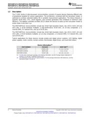
• Section 3 Summarizes Available Family Members
• Available in 40-Pin QFN (RSB), 38-Pin TSSOP
(DA), and 40-Pin Die-Sized BGA (YFF) Packages
• For Complete Module Descriptions, See the
MSP430x5xx and MSP430x6xx Family User's
Guide
1.2 Applications
• Analog and Digital Sensor Systems
• LED Lighting
• Digital Power Supplies
• Motor Controls
• Remote Controls
• Thermostats
Verzeichnis
- ・ Konfiguration des Pinbelegungsdiagramms on Seite 9 Seite 75 Seite 76 Seite 78 Seite 79
- ・ Abmessungen des Paketumrisses on Seite 7 Seite 105 Seite 106 Seite 107 Seite 108
- ・ Markierungsinformationen on Seite 98 Seite 105 Seite 106 Seite 107
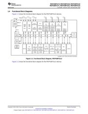
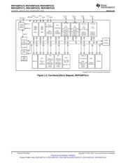
- ・ Blockdiagramm on Seite 3 Seite 4
- ・ Typisches Anwendungsschaltbild on Seite 2
- ・ Beschreibung der Funktionen on Seite 54
- ・ Technische Daten on Seite 14 Seite 15 Seite 16 Seite 17 Seite 18
- ・ Anwendungsbereich on Seite 1 Seite 117