
herunterladen
© Semiconductor Components Industries, LLC, 2008
August, 2016 − Rev. 11
1 Publication Order Number:
MC10EP16VA/D
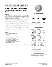
MC10EP16VA, MC100EP16VA
3.3V / 5V ECL Differential
Receiver/Driver with High
Gain
Description
The EP16VA is a world-class differential receiver/driver. The
device is functionally equivalent to the EP16 and LVEP16 devices but
with high gain output. Q
HG
and Q
HG
outputs have a DC gain several
times larger than the DC gain of an EP16.
The V
BB
pin, an internally generated voltage supply, is available to
this device only. For single-ended input conditions, the unused
differential input is connected to V
BB
as a switching reference voltage.
V
BB
may also rebias AC coupled inputs. When used, decouple V
BB
and V
CC
via a 0.01 mF capacitor and limit current sourcing or sinking
to 0.5 mA. When not used, V
BB
should be left open.
Under open input conditions (pulled to V
EE
) internal input clamps
will force the Q
HG
output LOW.
Special considerations are required for differential inputs under No
Signal conditions to prevent instability.
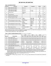
The 100 Series contains temperature compensation.
Features
• 270 ps Typical Propagation Delay
• Gain = > 20
• 20 mV Minimum Input Voltage Swing
• Maximum Frequency = > 3 GHz Typical
• PECL Mode Operating Range:
V
CC
= 3.0 V to 5.5 Vwith V
EE
= 0 V
• NECL Mode Operating Range:
V
CC
= 0 V with V
EE
= −3.0 V to −5.5 V
• Open Input Default State
• V
BB
Output
• These Devices are Pb-Free, Halogen Free and are RoHS Compliant
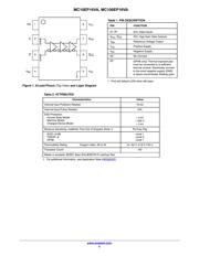
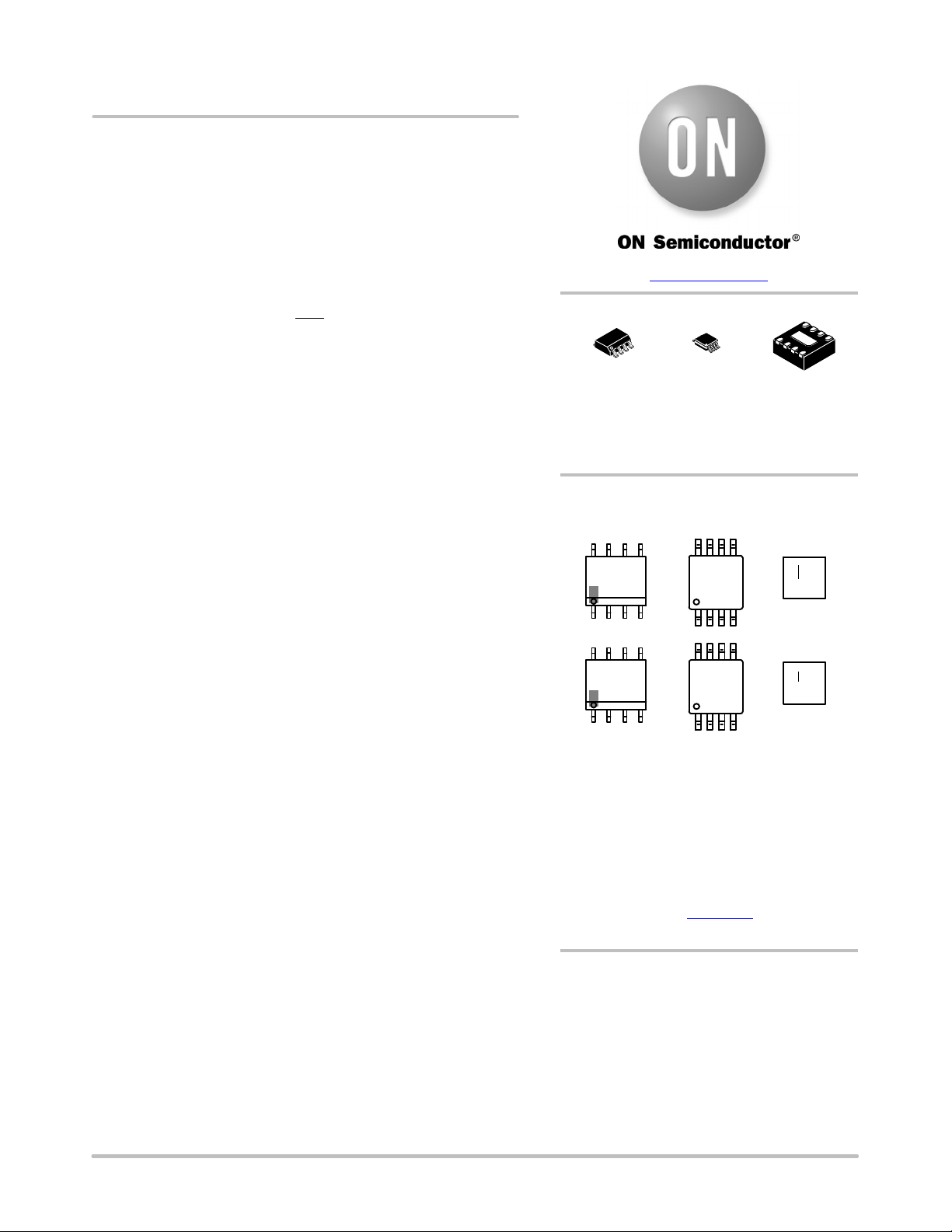
SOIC−8 NB
D SUFFIX
CASE 751−07
MARKING DIAGRAMS*
TSSOP−8
DT SUFFIX
CASE 948R−02
ALYWG
G
HP64
ALYWG
G
KP64
1
8
1
8
1
8
www.onsemi.com
*For additional marking information, refer to
Application Note AND8002/D
.
See detailed ordering and shipping information in the package
dimensions section on page 8 of this data sheet.
ORDERING INFORMATION
1
8
HEP64
ALYW
G
1
8
KEP64
ALYW
G
1
8
DFN8
MN SUFFIX
CASE 506AA
(Note: Microdot may be in either location)
SOIC−8 NB TSSOP−8 DFN8
A = Assembly Location
L = Wafer Lot
Y = Year
W = Work Week
G = Pb-Free Package
H = MC10
K = MC100
5M = MC10
3D = MC100
M = Date Code
5N MG
G
14
3E MG
G
14
Verzeichnis
- ・ Konfiguration des Pinbelegungsdiagramms on Seite 2
- ・ Abmessungen des Paketumrisses on Seite 9 Seite 10 Seite 11
- ・ Paket-Footprint-Pad-Layout on Seite 9 Seite 11
- ・ Teilenummerierungssystem on Seite 1 Seite 8 Seite 11
- ・ Markierungsinformationen on Seite 1 Seite 8 Seite 11
- ・ Typisches Anwendungsschaltbild on Seite 2
- ・ Technische Daten on Seite 8
- ・ Teilenummernliste on Seite 3