
herunterladen

www.latticesemi.com 1 tn1257_01.3
October 2013 Technical Note TN1257
© 2013 Lattice Semiconductor Corp. All Lattice trademarks, registered trademarks, patents, and disclaimers are as listed at www.latticesemi.com/legal. All other brand
or product names are trademarks or registered trademarks of their respective holders. The specifications and information herein are subject to change without notice.
Introduction
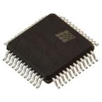
This document provides general PCB layout guidance for Lattice QFP (Quad Flat Package) and QFN (Quad Flat
No Lead) products. Table 1 below lists the common nomenclature for different types of packages. As it is antici-
pated that users may have specific PCB design rules and requirements, the recommendations made herein should
be considered as reference guidelines only.
When designing a PCB for a QFN or QFP package, the following primary factors can affect the successful package
mounting on the board:
• Perimeter Land Pad and Trace Design
• Stencil design
• Type of vias
• Board thickness
• Lead finish on the package
• Surface finish on the board
• Type of solder paste
• Reflow profile
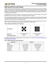
Table 1. Leaded Package Types
Package Type Description
QFN Quad Flat No Lead. Plastic package with flat lead frame base coplanar along its bottom side.
DR-QFN Dual Row-Quad Flat No Lead. QFN package that has two row staggered contacts.
QFP Quad Flat Package. Plastic package with “gull wing” leads extending from four sides of the body.
PQFP Plastic Quad Flat Package. QFP with body thickness from 2.0mm and above.
TQFP Thin Quad Flat Package. QFP with thin body profile typical at 1.40mm and 1.0mm.
PCB Layout Recommendations
for Leaded Packages
Verzeichnis