

herunterladen

User's Guide
SDLU003–July 2014
LSF010XEVM-001
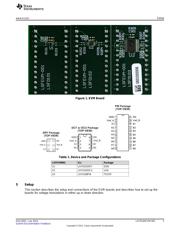
This document is the user's guide for the LSF010XEVM-001 Evaluation Module (EVM). The EVM allows
for evaluation of the different ways that the LSF devices can be used to translate voltages between 1 V
and 5.5 V.
Contents
1 About This Manual........................................................................................................... 2
2 Information About Cautions and Warnings............................................................................... 2
3 Items Required for Operation .............................................................................................. 2
4 Introduction ................................................................................................................... 2
5 Setup .......................................................................................................................... 3
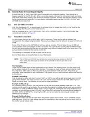
5.1 General Rules for Good Signal Integrity......................................................................... 4
6 Schematic..................................................................................................................... 6
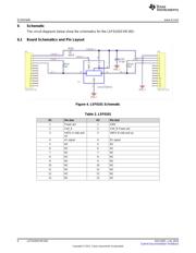
6.1 Board Schematics and Pin Layout ............................................................................... 6
7 B Board Layout............................................................................................................... 9
8 Bill of Materials (BOM)..................................................................................................... 10
List of Figures
1 EVM Board ................................................................................................................... 3
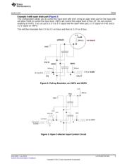
2 Pull-up Resistors on VAPU and VBPU ................................................................................... 5
3 Open Collector Input Control Circuit ...................................................................................... 5
4 LSF0101 Schematic......................................................................................................... 6
5 LSF0102 Schematic......................................................................................................... 7
6 LSF0108 Schematic......................................................................................................... 8
7 PCB Layer 1 (Top Layer)................................................................................................... 9
8 PCB (Bottom Layer)......................................................................................................... 9
List of Tables
1 Device and Package Configurations ...................................................................................... 3
2 LSF0101 ...................................................................................................................... 6
3 LSF0102 ...................................................................................................................... 7
4 LSF0108 ...................................................................................................................... 8
5 Bill of Materials ............................................................................................................. 10
1
SDLU003–July 2014 LSF010XEVM-001
Submit Documentation Feedback
Copyright © 2014, Texas Instruments Incorporated
Verzeichnis
- ・ Blockdiagramm on Seite 6 Seite 7 Seite 8
- ・ Anwendungsbereich on Seite 11