
herunterladen
User's Guide
SNOA429–May 2004
AN-1268 LP2996 Evaluation Board
1 Introduction
The LP2996 evaluation board is designed to provide the design engineer with a fully functional prototype
system in which to evaluate the LP2996 in both a static environment and with a complete memory system.
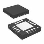
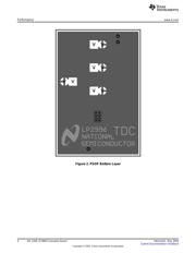
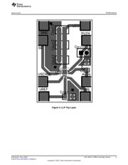
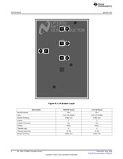
There are two versions of the board, and while identical in functionality they differ in the package
implemented; either a PSOP-8 or LLP-16 is used. This application note contains information regarding the
board. For more information regarding the LP2996 please refer to the datasheet.
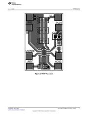
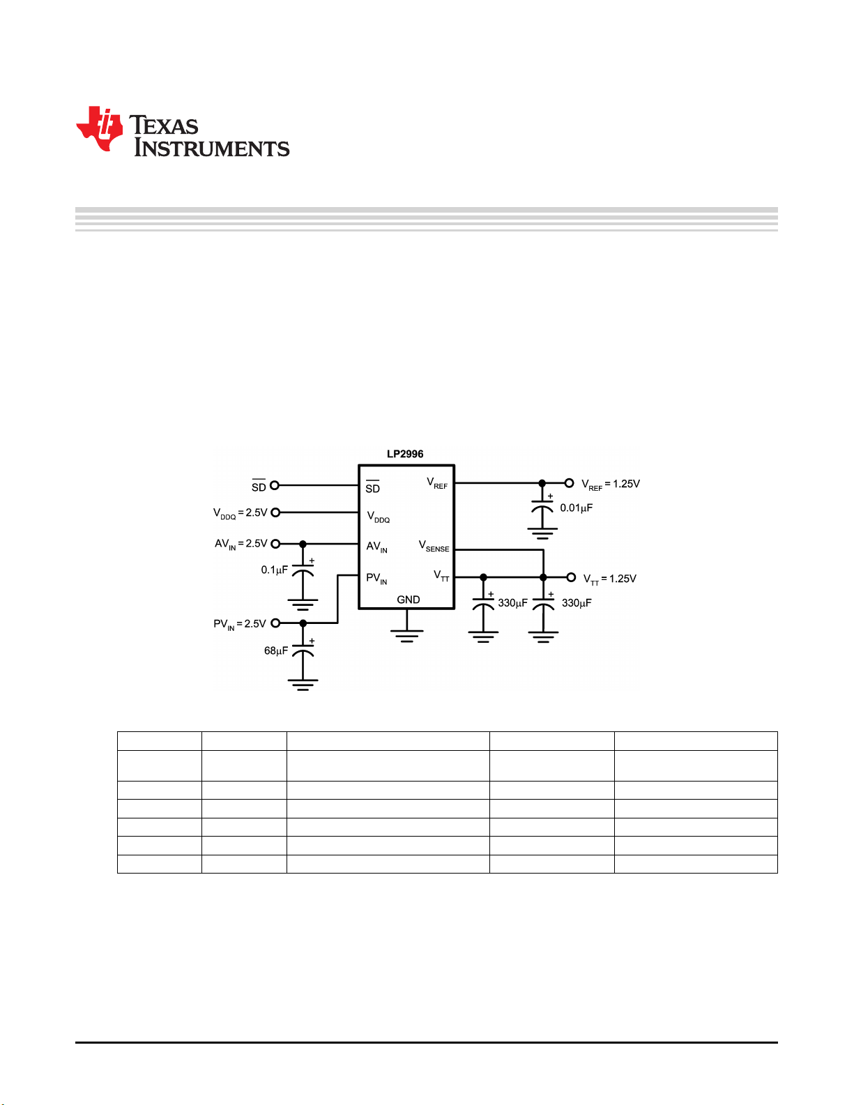
2 Schematic
The following schematic was used to create the layout.
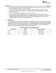
Table 1. Bill of Materials
Name Value Description Manufacturer Model Number
LP2996 DDR Linear Regulator National LP2996MR or LP2996LQ
U1
Semiconductor
CAVIN 0.1µF 1206 Ceramic Capacitor X7R 25V Vishay Vitrammon VJ1206Y104KXXAT
COUT1 330µF 6.3V Electrolytic Radial FC Series Panasonic EEU-FC0J331S
COUT2 330µF 6.3V Electrolytic Radial FC Series Panasonic EEU-FC0J331S
CREF 0.01µF 1206 Ceramic Capacitor X7R 25V Vishay Vitrammon VJ1206Y103KXXAT
CPVIN 68µF 6.3V Electrolytic Radial FC series Panasonic EEU-FC0J680
3 Application
The LP2996 evaluation board can be used immediately in either a static test environment to check
functionality, or in a memory termination scheme on a motherboard. In either implementation, the following
steps should be taken to ensure correct operation.
1. Connect leads from the evaluation board. The board layout has been designed to allow banana jack
sockets to be directly soldered.
2. Connect AVIN and PVIN to a 2.5V power supply.
1
SNOA429–May 2004 AN-1268 LP2996 Evaluation Board
Submit Documentation Feedback
Copyright © 2004, Texas Instruments Incorporated
Verzeichnis
- ・ Blockdiagramm on Seite 1
- ・ Anwendungsbereich on Seite 7