

herunterladen
Application Report
SNVA499E–July 2011–Revised May 2013
AN-2178 LM5118 Four Switch Conversion
.....................................................................................................................................................
ABSTRACT
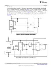
This application note discusses the conversion of the LM5118 Buck-Boost Controller from a two-switch
version to a fully synchronous four-switch version.
Contents
1 Introduction .................................................................................................................. 2
2 Applications Information .................................................................................................... 3
3 Air Flow ....................................................................................................................... 3
4 Design Details ............................................................................................................... 3
5 Precautions .................................................................................................................. 3
6 Results ....................................................................................................................... 4
7 PCB Layout .................................................................................................................. 6
8 Schematic Diagram ......................................................................................................... 8
9 Bill of Materials .............................................................................................................. 9
List of Figures
1 Two Switch Simplified Block Diagram.................................................................................... 2
2 Four Switch Simplified Block Diagram ................................................................................... 2
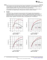
3 8V Input ...................................................................................................................... 4
4 18 V Input.................................................................................................................... 4
5 36 V Input.................................................................................................................... 4
6 48 V Input.................................................................................................................... 4
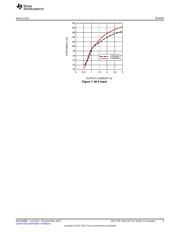
7 60 V Input.................................................................................................................... 4
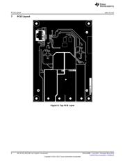
8 Top PCB Layer.............................................................................................................. 6
9 Bottom PCB Layer.......................................................................................................... 7
10 Schematic Diagram......................................................................................................... 8
List of Tables
1 Bill of Materials.............................................................................................................. 9
All trademarks are the property of their respective owners.
1
SNVA499E–July 2011–Revised May 2013 AN-2178 LM5118 Four Switch Conversion
Submit Documentation Feedback
Copyright © 2011–2013, Texas Instruments Incorporated
Verzeichnis
- ・ Blockdiagramm on Seite 2 Seite 8
- ・ Anwendungsbereich on Seite 3 Seite 11