
herunterladen

User's Guide
SNVA203C–January 2007–Revised May 2013
AN-1557 LM5022 Evaluation Board
The AN-1557 is an evaluation module that demonstrates a typical 20W Boost converter featuring the
LM5022 60V low-side controller in a design that shows high efficiency in a single-ended application.
Contents
1 Specifications Of The Board ............................................................................................... 2
2 Example Circuit .............................................................................................................. 2
3 Powering The Converter ................................................................................................... 2
4 Loading The Converter ..................................................................................................... 2
5 Enabling The Converter .................................................................................................... 2
6 Testing The Converter ..................................................................................................... 3
7 MOSFET Footprints ........................................................................................................ 3
8 Permanent Components ................................................................................................... 4
9 Additional Footprints ........................................................................................................ 4
10 Typical Performance Characteristics ..................................................................................... 6
11 Bill of Materials .............................................................................................................. 8
12 PC Board Layout ............................................................................................................ 9
List of Figures
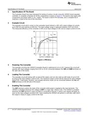
1 Efficiency..................................................................................................................... 2
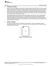
2 SO-8 MOSFET Pinout...................................................................................................... 3
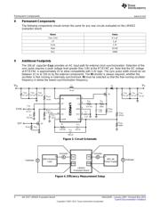
3 Circuit Schematic ........................................................................................................... 4
4 Efficiency Measurement Setup............................................................................................ 4
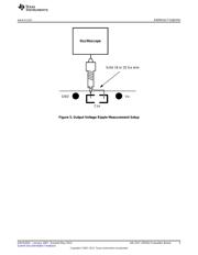
5 Output Voltage Ripple Measurement Setup............................................................................. 5
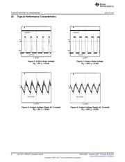
6 Switch Node Voltage (V
IN
= 9V, I
O
= 0.5A)............................................................................... 6
7 Switch Node Voltage (V
IN
= 16V, I
O
= 0.5A) ............................................................................. 6
8 Output Voltage Ripple AC Coupled (V
IN
= 9V, I
O
= 0.5A).............................................................. 6
9 Output Voltage Ripple AC Coupled (V
IN
= 16V, I
O
= 0.5A) ............................................................ 6
10 Load Transient Response (V
IN
= 9V, I
O
= 50 mA to 0.5A) ............................................................. 6
11 Load Transient Response (V
IN
= 16V, I
O
= 50 mA to 0.5A)............................................................ 6
12 Start Up (V
IN
= 9V, I
O
= 0.5A).............................................................................................. 7
13 Shut Down (V
IN
= 9V, I
O
= 0.5A)........................................................................................... 7
14 Start Up (V
IN
= 16V, I
O
= 0.5A) ............................................................................................ 7
15 Shutdown (V
IN
= 16V, I
O
= 0.5A) .......................................................................................... 7
16 NGATE Rise Time (V
IN
= 9V, I
O
= 0.1A, Si4850DY).................................................................... 7
17 NGATE Fall Time (V
IN
= 12V, I
O
= 0.1A, Si4850DY) ................................................................... 7
18 Top Layer and Top Overlay ............................................................................................... 9
19 Bottom Layer ................................................................................................................ 9
All trademarks are the property of their respective owners.
1
SNVA203C–January 2007–Revised May 2013 AN-1557 LM5022 Evaluation Board
Submit Documentation Feedback
Copyright © 2007–2013, Texas Instruments Incorporated
Verzeichnis
- ・ Blockdiagramm on Seite 4
- ・ Technische Daten on Seite 2
- ・ Anwendungsbereich on Seite 10
- ・ Elektrische Spezifikation on Seite 6 Seite 7