
herunterladen
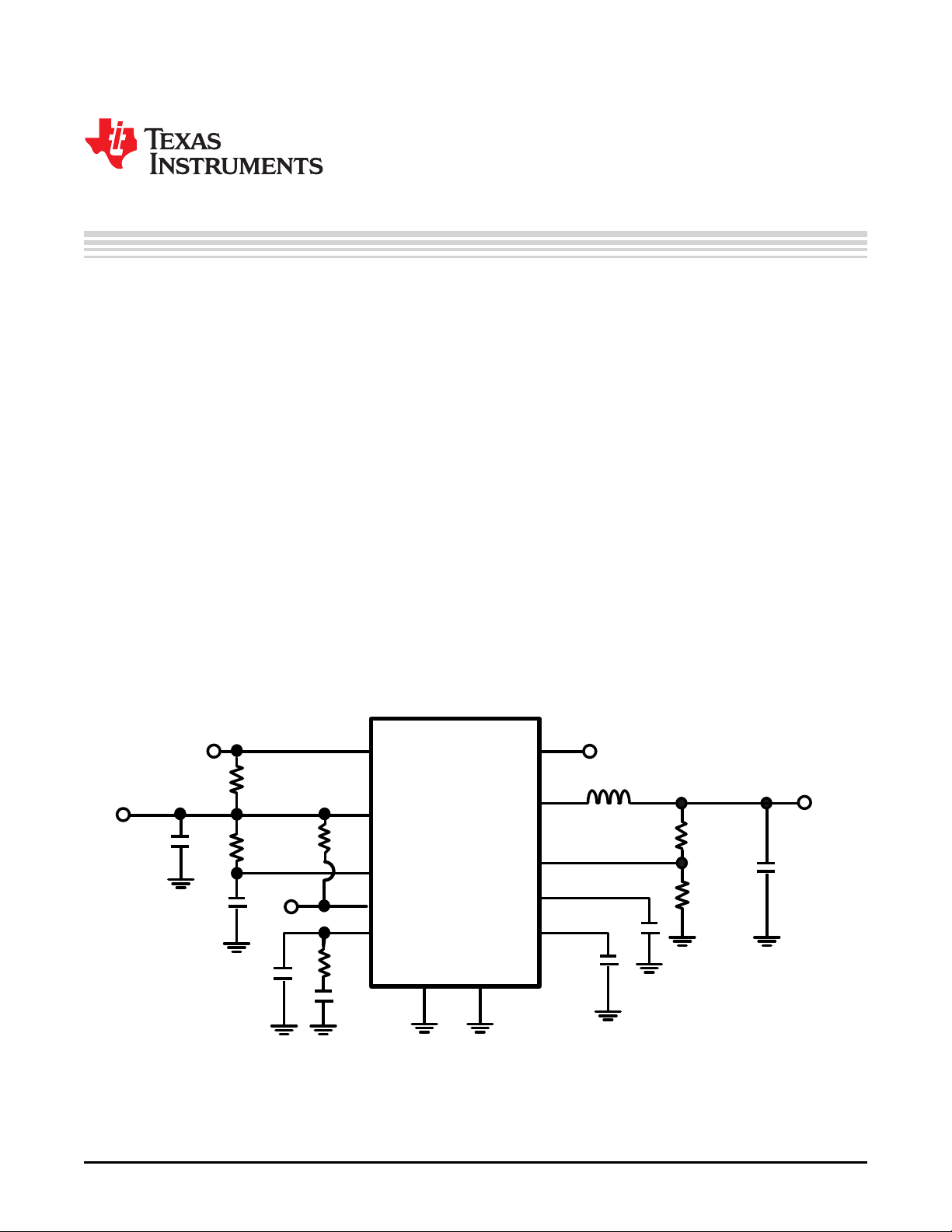
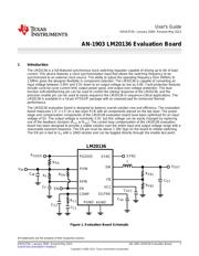
PVIN
SW
AGND
FB
PGOOD
R
FB1
R
FB2
C
O1
EN
C
SS
SS/TRK
AVIN
C
F
C
C1
COMP
R
C1
V
IN
LM20136
L
R
F
VCC
C
VCC
V
OUT
PGND
P
GOOD
R
PG
EN
C
C2
SYNC
SYNC
C
IN
R
EN
User's Guide
SNVA373A–January 2009–Revised May 2013
AN-1903 LM20136 Evaluation Board
1 Introduction
The LM20136 is a full-featured synchronous buck switching regulator capable of driving up to 6A of load
current. This device features a clock synchronization input that allows the switching frequency to be
synchronized to an external clock source. The ability to adjust the operating frequency from 500kHz to
1.5MHz gives the designer flexibility in component selection. The LM20136 is capable of converting an
input voltage between 2.95V and 5.5V down to an output voltage as low as 0.8V. Fault protection features
include cycle-by-cycle current limit, output power good, and output over-voltage protection. The dual
function soft-start/tracking pin can be used to control the startup response of the LM20136, and the
precision enable pin can be used to easily sequence the LM20136 in sequence-critical applications. The
LM20136 is available in a 16-pin HTSSOP package with an exposed pad for enhanced thermal
performance.
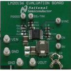
The LM20136 evaluation board is designed to balance overall solution size and efficiency. The evaluation
board measures 1.5” × 1.5” on a two layer PCB with all components placed on the top layer. The power
stage and compensation components of the LM20136 evaluation board have been optimized for an input
voltage of 5V. The output voltage is nominally 3.3V, but this voltage can be easily changed by replacing
one of the feedback resistors (R
FB1
or R
FB2
). The control loop compensation of the LM20136 evaluation
board has been designed to provide a stable solution over the entire input and output voltage range with a
reasonable transient response. The EN pin must be above 1.18V (typ) on the board to initiate switching.
The EN pin is tied to V
IN
with a 10kΩ resistor and can be toggled directly through the enable test point.
Figure 1. Evaluation Board Schematic
All trademarks are the property of their respective owners.
1
SNVA373A–January 2009–Revised May 2013 AN-1903 LM20136 Evaluation Board
Submit Documentation Feedback
Copyright © 2009–2013, Texas Instruments Incorporated
Verzeichnis
- ・ Blockdiagramm on Seite 1
- ・ Anwendungsbereich on Seite 8
- ・ Elektrische Spezifikation on Seite 6