


herunterladen

Developer's Guide
SLLA284A–January 2009–Revised November 2014
Digital Isolator Design Guide
This design guide helps system designers of galvanically isolated systems to begin designing with TI's
broad portfolio of digital isolators and isolated functions in the shortest time possible. This portfolio
includes the ISO78xx family of 5.7-kVrms reinforced digital isolators, the ISO73xx family of 3-kVrms digital
isolators, and the ISO71xx family of 2.5-kVrms digital isolators, among others. This document explains the
basic operating principle of an isolator, suggests where to place it within a system design, and
recommends guidelines for an electromagnetic compatible (EMC) circuit-board design.
Further information is available in the respective product data sheets and the EVM manuals.
Contents
1 Operating Principle .......................................................................................................... 2
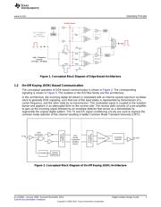
1.1 Edge-Based Communication...................................................................................... 2
1.2 On-Off Keying (OOK) Based Communication................................................................... 3
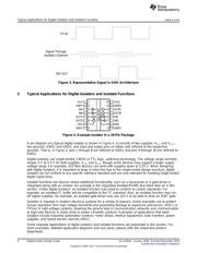
2 Typical Applications for Digital Isolators and Isolated Functions...................................................... 4
3 Digital Isolator Selection Guide ............................................................................................ 6
3.1 Parameters of Interest ............................................................................................. 6
3.2 Isolator Families..................................................................................................... 7
4 PCB Design Guidelines..................................................................................................... 8
4.1 PCB Material ........................................................................................................ 8
4.2 Layer Stack.......................................................................................................... 8
4.3 Creepage Distance ................................................................................................. 8
4.4 Controlled Impedance Transmission Lines...................................................................... 9
4.5 Reference Planes ................................................................................................. 11
4.6 Routing ............................................................................................................. 12
4.7 Vias.................................................................................................................. 14
4.8 Decoupling Capacitors............................................................................................ 16
5 Summary .................................................................................................................... 17
6 References.................................................................................................................. 17
List of Figures
1 Conceptual Block Diagram of Edge-Based Architecture ............................................................... 3
2 Conceptual Block Diagram of On-Off Keying (OOK) Architecture .................................................... 3
3 Representative Signal in OOK Architecture.............................................................................. 4
4 Example Isolator in a 16-Pin Package.................................................................................... 4
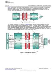
5 Isolated SPI Interface ....................................................................................................... 5
6 Isolated RS-232 Interface................................................................................................... 5
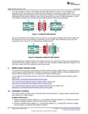
7 Isolated RS-485 Interface................................................................................................... 6
8 Integrated Isolated RS-485 Interface...................................................................................... 6
9 Recommended Layer Stack................................................................................................ 8
10 Groove Cutting Extends Effective Creepage Distance ................................................................. 9
11 Source Impedance Matching: Z
0
~ r
O
..................................................................................... 9
12 Isolator Output Characteristic............................................................................................. 10
13 Characteristic Impedance as a Function of the w/h Ratio ............................................................ 10
14 Reducing Field Fringing Through Close Electric Coupling Between Conductors.................................. 11
15 Ground Plane Acting as a Single Return Trace........................................................................ 12
1
SLLA284A–January 2009–Revised November 2014 Digital Isolator Design Guide
Submit Documentation Feedback
Copyright © 2009–2014, Texas Instruments Incorporated
Verzeichnis