
herunterladen
FN7462 Rev 0.00 Page 1 of 13
October 13, 2005
FN7462
Rev 0.00
October 13, 2005
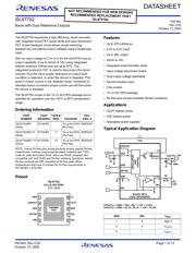
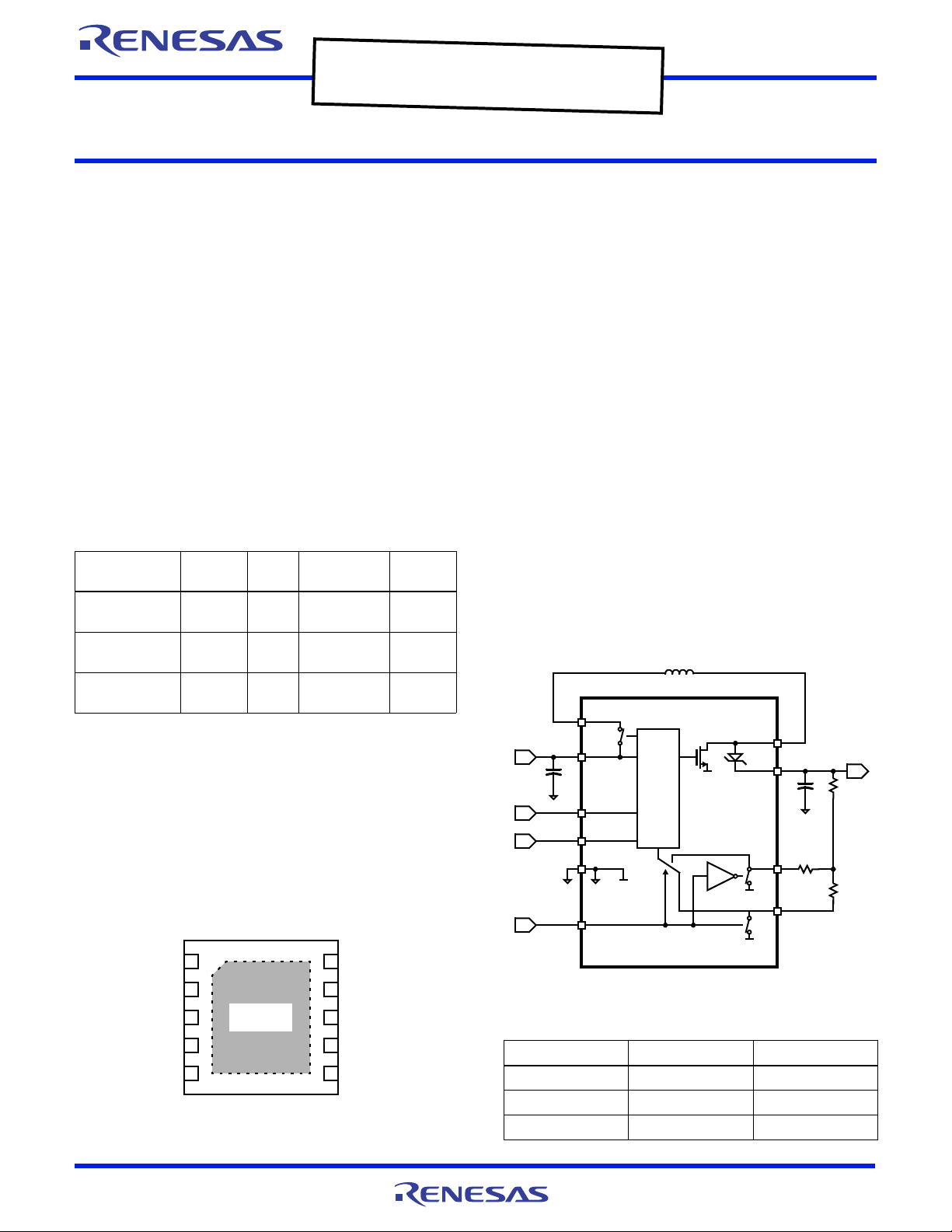
ISL97702
Boost with Dual Reference Outputs
DATASHEET
The ISL97702 represents a high efficiency, boost converter
with integrated boost FET, boost diode and input disconnect
FET. A dual feedback circuit allows simple switching
between two pre-defined output voltages using a single logic
input.
With an input voltage of 2.3V to 5.5V the ISL97702 has an
output capability of up to 50mA at 18V using integrated
500mA switches. Efficiencies are up to 87%. The
integrated protection FET is used to disconnect the boost
inductor from the input supply whenever an output fault
condition is detected, or when the device is disabled. This
gives 0 output current in the disabled mode, compared to
standard boost converters where current can still flow when
the device is disabled.
The ISL97702 comes in the 10 Ld 3x3 DFN package and is
specified for operation over the -40°C to 85°C temperature
range.
Pinout
ISL97702
(10 LD 3X3 DFN)
TOP VIEW
Features
• Up to 87% efficiency
• 2.3V to 5.5V input
• Up to 28V output
• 50mA at 18V
• Integrated boost Schottky diode
• Input voltage disconnect switch
• Dual output voltage selectable
• Synchronization input
• Chip enable
• 10 Ld 3x3 DFN package
• Pb-free plus anneal available (RoHS compliant)
Applications
• OLED display power
• LED display power
• Adjustable power supplies
Typical Application Diagram
Ordering Information
PART
NUMBER
PART
MARKING
TAPE &
REEL PACKAGE
PKG.
DWG. #
ISL97702IRZ
(Note)
97702IRZ - 10 Ld 3x3 DFN
(Pb-Free)
MDP0047
ISL97702IRZ-T7
(Note)
97702IRZ 7” 10 Ld 3x3 DFN
(Pb-Free)
MDP0047
ISL97702IRZ-T13
(Note)
97702IRZ 13” 10 Ld 3x3 DFN
(Pb-Free)
MDP0047
NOTE: Intersil Pb-free plus anneal products employ special Pb-free
material sets; molding compounds/die attach materials and 100%
matte tin plate termination finish, which are RoHS compliant and
compatible with both SnPb and Pb-free soldering operations. Intersil
Pb-free products are MSL classified at Pb-free peak reflow
temperatures that meet or exceed the Pb-free requirements of
IPC/JEDEC J STD-020.
1
2
3
4
10
9
8
7
5 6
THERMAL
PAD
GND
VDDOUT
VDD
NSYNC
LX
VOUT
NEN
SEL
FB1
FB0
NEN SEL V
OUT
1XHigh Z
00V
OUT0
01V
OUT1
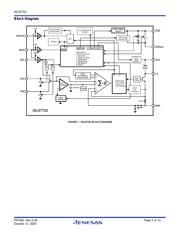
OSCILLATOR
AND
CONTROL
VDDOUT
NEN
NSYNC
GND
SEL
C
0
5µ
C
1
3.3µ
R
1
390k
R
2
39k
R
3
26.1k
L
1
6.8µ
LX
VOUT
FB0
FB1
BOOST WITH
DUAL REFERENCE
V
DD
+2V - 30V
V(VOUT)
0
= (390k + 39k) / 39k * 1.15V = 12.65V
V(VOUT)
1
= (390k + 26.1k) / 26.1k * 1.15V = 18.33V
VDD
2.3V-5.5V
N
O
T
R
E
C
O
M
M
E
N
D
E
D
F
O
R
N
E
W
D
E
S
I
G
N
S
R
E
C
O
M
M
E
N
D
E
D
R
E
P
L
A
C
E
M
E
N
T
P
A
R
T
I
S
L
9
7
5
1
9
A
Verzeichnis
- ・ Konfiguration des Pinbelegungsdiagramms on Seite 8
- ・ Teilenummerierungssystem on Seite 1
- ・ Markierungsinformationen on Seite 1
- ・ Blockdiagramm on Seite 2
- ・ Typisches Anwendungsschaltbild on Seite 1 Seite 11
- ・ Technische Daten on Seite 4
- ・ Anwendungsbereich on Seite 1 Seite 11
- ・ Elektrische Spezifikation on Seite 4