
herunterladen
1
®
AN1273.2
CAUTION: These devices are sensitive to electrostatic discharge; follow proper IC Handling Procedures.
1-888-INTERSIL or 1-888-468-3774
| Intersil (and design) is a registered trademark of Intersil Americas Inc.
Copyright Intersil Americas Inc. 2006, 2007. All Rights Reserved
All other trademarks mentioned are the property of their respective owners.
ISL6269AEVAL2Z User Guide For ISL6269A and
ISL6269B PWM Controllers
Introduction
The ISL6269AEVAL2Z evaluation board demonstrates the
performance of the ISL6269A or ISL6269B single-phase
synchronous-buck PWM controller featuring Intersil's Robust
Ripple Regulator (R
3
) technology. The ISL6269AEVAL2Z is
shipped with the ISL6269A controller installed. The
ISL6269B controller can be evaluated using the
ISL6269AEVAL2Z with no further circuit modifications
beyond changing the IC. An on-board dynamic-load
generator is included for evaluating the transient-load
response, that applies a 2.5ms pulse of 250mΩ across
V
OUT
and GND every 30ms. Contents of this document
include:
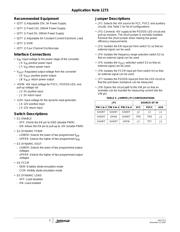
• Design Criteria
• Recommended Test Equipment
• Interface Connections
• Switch Descriptions
• Jumper Descriptions
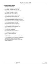
• Test Point Descriptions
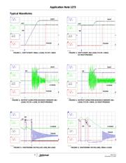
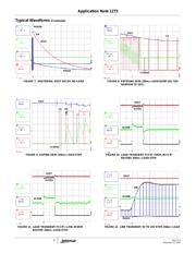
• Typical Waveforms
- Start-up
- Shut-down
- Diode-emulation
- Load-transient response
- Line-transient response
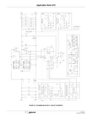
• Evaluation Board Documentation
- Schematic
- Bill of materials
- Silk-screen plots
- Board layer plots
Design Criteria
The design criteria listed in Table 1 was, to a large extent,
influenced by customer input. The PWM switching frequency
can be programmed to any frequency between 200kHz and
600kHz. If only one PWM frequency setting is desired, this
can be accomplished by simply not populating R
17
. The
output voltage can be programmed to any voltage between
0.6V and 3.3V. If only one output voltage setting is desired,
this can be accomplished by simply not populating R
16
.
The OCP setpoint resistor R
SEN
(R
13
) is selected to protect
the output load, without nuisance shutdowns due to
component tolerances and temperature effects. Using
Equation 1 finds R
SEN
(R
13
) = 6.49kΩ where:
-r
DS(ON)
of Q4 low-side MOSFETs is 15mΩ
-I
OC
is 26µA
-I
FL
is 5A continuous
-I
PP
is 1.5A
PP
(30% of I
FL
5A)
-OC
SP
is 2.1 (210% of I
FL
)
The PWM switching frequency f
SW
is programmed for
300kHz by resistance R
FSET
(R
12
) when switch S2 is in the
LOWER position. Setting switch S2 in the UPPER position
will program f
SW
for approximately 600kHz with the parallel
resistance of R
12
and R
17
. Using Equation 2 finds the value
for R
FSET
(R
12
) = 57.6kΩ. The “K” constant in Equation 2 is
ideally 66.8 x 10
-12
however, this value can be affected by
the ripple voltage on the COMP pin. The ripple voltage on
the COMP pin increases with the bandwidth of the feedback
loop compensation, effectively reducing the value of “K”. The
ISL6269AEVAL2Z evaluation board is aggressively
compensated for approximately 100kHz bandwidth, making
the value of “K” effectively 58 x 10
-12
.
The output voltage is programmed for 1.10V using resistors
R
19
(R
TOP
) and R
20
(R
BOTTOM
) when switch S3 is in the
LOWER position. Setting switch S3 in the UPPER position
will program the output voltage for 1.20V using resistor R
19
(R
TOP
) and the parallel resistance of R
20
and R
16
(R
BOTTOM
). The loop compensation is usually responsible
for selecting R
TOP
(R19), which in this case is 3.01kΩ. The
voltage setpoint programming resistance R
BOTTOM
is
calculated using Equation 3 where:
-V
REF
= 600mV
-R
TOP
= 3.01kΩ
-V
OUT
= 1.10V or 1.20V
Begin by finding the value of R
20
for V
OUT
= 1.10V from
Equation 2: R
20
= 3.57kΩ. Find the value of parallel
resistance R
20
and R
16
for V
OUT
= 1.20V from Equation 3:
R
20
||R
16
= 3.01kΩ, therefore R
16
= 19.1kΩ.
TABLE 1. DC/DC DESIGN CRITERIA
PARAMETER VALUE UNITS
VIN 5 to 25 VDC
VOUT 1.10 or 1.20 VDC
FULL-LOAD 5.0 ADC
PWM FREQUENCY 300 or 600 kHz
(EQ. 1)
R
SEN
I
FL
I
PP
2
---------
+
⎝⎠
⎛⎞
OC
SP
• r
DS ON()
•
I
OC
----------------------------------------------------------------------------
=
R
FSET
1
Kf
SW
•
------------------
=
(EQ. 2)
R
BOTTOM
V
REF
R
TOP
⋅()
V
OUT
V
REF
–()
------------------------------------------
=
(EQ. 3)
Application Note November 14, 2007