
herunterladen

Order On-line at www.analog.com/hittitemw
For technical application questions: Phone: 978-250-3343 or RFMG-pll@analog.com
Product & oPerating guide
a
A - 1
PLLs WITH INTEGRATED VCO - RF APPLICATIONS
PRODUCT & OPERATING GUIDE
v12.1215
Table of Contents
1.0 Applicable Products .......................................................4
2.0 General Description. . . . . . . . . . . . . . . . . . . . . . . . . . . . . . . . . . . . . . . . . . . . . . . . . . . . . . . . 4
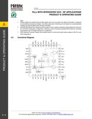
3.0 Functional Diagram . . . . . . . . . . . . . . . . . . . . . . . . . . . . . . . . . . . . . . . . . . . . . . . . . . . . . . . . 5
4.0 Theory of Operation .......................................................6
4.1 VCO Subsystem ...........................................................6
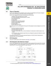
4.1.1 VCO Subsystem with Divide-by-2 Output . . . . . . . . . . . . . . . . . . . . . . . . . . . . . . . . . . . . . . 6
4.1.2 VCO Subsystem with Fundamental Output ....................................7
4.1.3 VCO Subsystem with Doubler Output . . . . . . . . . . . . . . . . . . . . . . . . . . . . . . . . . . . . . . . . . 7
4.1.4 VCO Subsystem with Tri-band Output. . . . . . . . . . . . . . . . . . . . . . . . . . . . . . . . . . . . . . . . . 8
4.1.5 VCO Subsystem with Wideband Output .......................................8
4.2 VCO Calibration ...........................................................9
4.2.1 VCO Auto-Calibration (AutoCal). . . . . . . . . . . . . . . . . . . . . . . . . . . . . . . . . . . . . . . . . . . . . . 9
4.2.1.1 AutoCal Use of Reg05h . . . . . . . . . . . . . . . . . . . . . . . . . . . . . . . . . . . . . . . . . . . . . . . . . . . . 10
4.2.1.2 Auto-reLock on Lock Detect Failure .........................................10
4.2.2 Manual VCO Calibration ...................................................10
4.2.2.1 Registers required for Frequency Changes in Fractional Mode ..................11
4.2.2.2 Registers Required for Frequency Changes in Integer Mode ....................11
4.2.3 VCO AutoCal on Frequency Change .........................................11
4.2.4 VCO AutoCal Time & Accuracy .............................................11
4.2.4.1 VCO AutoCal Example. . . . . . . . . . . . . . . . . . . . . . . . . . . . . . . . . . . . . . . . . . . . . . . . . . . . . 13
4.3 VCO Built in Test with AutoCal ..............................................13
4.4 Spurious Performance ....................................................14
4.4.1 Integer Operation and Reference Spurious ...................................14
4.4.2 Fractional Operation and Spurious ..........................................14
4.4.2.1 Charge Pump and Phase Detector Spurious Considerations. . . . . . . . . . . . . . . . . . . . . 15
4.4.2.2 Spurious Related to Channel Step Size (Channel Spurs) ........................16
4.4.2.3 Spurious Reduction with Tunable Reference ..................................16
4.5 Integrated Phase Noise & Jitter . . . . . . . . . . . . . . . . . . . . . . . . . . . . . . . . . . . . . . . . . . . . . 18
4.6 Reference Input Stage. . . . . . . . . . . . . . . . . . . . . . . . . . . . . . . . . . . . . . . . . . . . . . . . . . . . . 20
4.7 Reference Path ’R’ Divider .................................................21
4.8 RF Path ’N’ Divider .......................................................21
4.9 Charge Pump & Phase Detector. . . . . . . . . . . . . . . . . . . . . . . . . . . . . . . . . . . . . . . . . . . . . 21
4.10 Phase Detector Functions .................................................21
4.11 Phase Detector Window Based Lock Detect ..................................21
4.11.1 Analog Window Lock Detect ...............................................21
4.11.2 Digital Window Lock Detect ................................................22
4.11.3 Declaration of Lock . . . . . . . . . . . . . . . . . . . . . . . . . . . . . . . . . . . . . . . . . . . . . . . . . . . . . . . 22
4.11.4 Phase Offset & Fractional Linearity ..........................................23
4.11.5 Digital Lock Detect with Digital Window Example ..............................23
4.11.6 Cycle Slip Prevention (CSP) . . . . . . . . . . . . . . . . . . . . . . . . . . . . . . . . . . . . . . . . . . . . . . . . 24
4.11.7 Charge Pump Gain. . . . . . . . . . . . . . . . . . . . . . . . . . . . . . . . . . . . . . . . . . . . . . . . . . . . . . . . 25
4.11.8 Charge Pump Phase Offset - Fractional Mode . . . . . . . . . . . . . . . . . . . . . . . . . . . . . . . . . 25
4.12 Frequency Tuning ........................................................26
4.12.1 Integer Mode ............................................................26
Verzeichnis