
herunterladen
8-Channel, 12-Bit, Configurable ADC/DAC
with On-Chip Reference, SPI Interface
Data Sheet
AD5592R
Rev. B
Document Feedback
Information furnished by Analog Devices is believed to be accurate and reliable. However, no
responsibility is assumed by Analog Devices for its use, nor for any infringements of patents or other
rights of third parties that may result from its use. Specifications subject to change without notice. No
license is granted by implication or otherwise under any patent or patent rights of Analog Devices.
Trademarks and registered trademarks are the property of their respective owners.
One Technology Way, P.O. Box 9106, Norwood, MA 02062-9106, U.S.A.
Tel: 781.329.4700 ©2014–2016 Analog Devices, Inc. All rights reserved.
Technical Support www.analog.com
FEATURES
8-channel, configurable ADC/DAC/GPIO
Configurable as any combination of
8 × 12-bit DAC channels
8 × 12-bit ADC channels
8 × general-purpose digital input/output pins
Integrated temperature sensor
SPI interface
Available in
16-ball, 2 mm × 2 mm WLCSP
16-lead, 3 mm × 3 mm LFCSP
16-lead TSSOP
APPLICATIONS
Control and monitoring
General-purpose analog and digital inputs/outputs
GENERAL DESCRIPTION
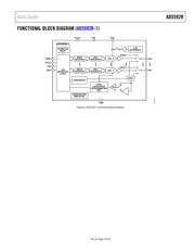
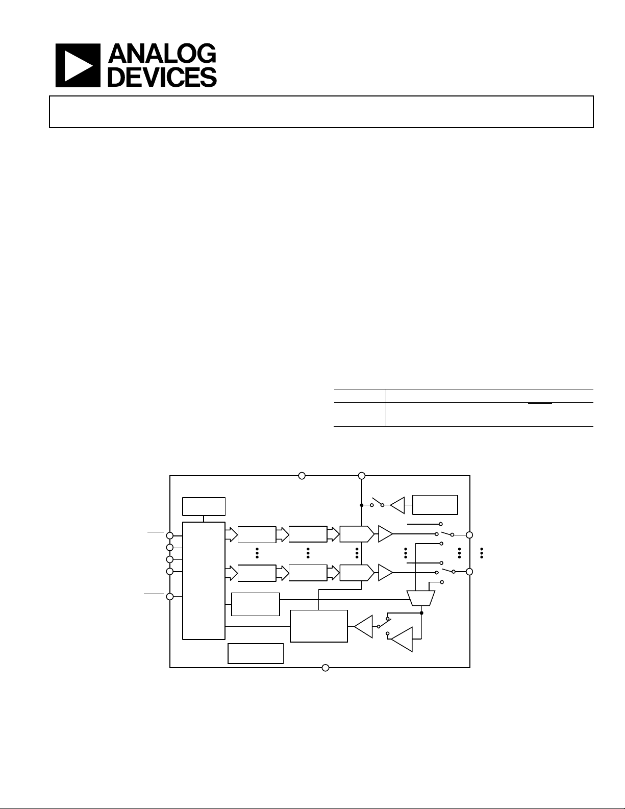
The AD5592R/AD5592R-1 have eight I/Ox pins (I/O0 to I/O7)
that can be independently configured as digital-to-analog
converter (DAC) outputs, analog-to-digital converter (ADC)
inputs, digital outputs, or digital inputs. When an I/Ox pin is
configured as an analog output, it is driven by a 12-bit DAC.
The output range of the DAC is 0 V to V
REF
or 0 V to 2 × V
REF
.
When an I/Ox pin is configured as an analog input, it is
connected to a 12-bit ADC via an analog multiplexer. The input
range of the ADC is 0 V to V
REF
or 0 V to 2 × V
REF
. The ADC
has a total throughput rate of 400 kSPS. The I/Ox pins can also
be configured as digital, general-purpose input or output
(GPIO) pins. The state of the GPIO pins can be set or read back
by accessing the GPIO write data register or the GPIO read
configuration register, respectively, via a serial peripheral
interface (SPI) write or read operation.
The AD5592R/AD5592R-1 have an integrated 2.5 V, 25 ppm/°C
reference, which is turned off by default, and an integrated
temperature indicator, which gives an indication of the die
temperature. The temperature value is read back as part of an
ADC read sequence.
The AD5592R/AD5592R-1 are available in 16-ball, 2 mm ×
2 mm WLCSP, 16-lead, 3 mm × 3 mm LFCSP, and 16-lead
TSSOP. The AD5592R/AD5592R-1 operate over a temperature
range of −40°C to +105°C.
Table 1. Related Products
Part No. Description
AD5593R AD5592R equivalent with V
LOGIC
and
RESET
pins and
an I
2
C interface
FUNCTIONAL BLOCK DIAGRAM
Figure 1. AD5592R Functional Block Diagram
RESET
V
REF
I/O7
I/O0
SYNC
GPIO7
GPIO0
T/H
SEQUENCER
V
DD
GND
SCLK
SDI
SDO
TEMPERATURE
INDICATOR
DAC
REGISTER
INPUT
REGISTER
DAC 7
DAC
REGISTER
INPUT
REGISTER
DAC 0
AD5592R
MUX
12-BIT
SUCCESSIVE
APPROXIMATION
ADC
POWER-ON
RESET
SPI
INTERFACE
LOGIC
2.5V
REFERENCE
12506-001
Verzeichnis
- ・ Konfiguration des Pinbelegungsdiagramms on Seite 10 Seite 11 Seite 12 Seite 13 Seite 14
- ・ Abmessungen des Paketumrisses on Seite 41
- ・ Teilenummerierungssystem on Seite 42
- ・ Blockdiagramm on Seite 1 Seite 3 Seite 23
- ・ Beschreibung der Funktionen on Seite 1 Seite 10 Seite 11 Seite 12 Seite 13
- ・ Technische Daten on Seite 1 Seite 4 Seite 5 Seite 8 Seite 9
- ・ Anwendungsbereich on Seite 1 Seite 40
- ・ Elektrische Spezifikation on Seite 15