
herunterladen
QUICK START GUIDE FOR DEMONSTRATION CIRCUIT 965A
SINGLE 5A HIGH FREQUENCY STEP-DOWN DC/DC CONVERTER
1
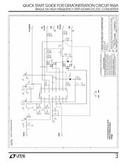
LTC3835EGN-1
DESCRIPTION
Demonstration circuit 965A is a single output high
frequency step-down DC/DC converter featuring the
low quiescent current LTC
®
3835 in a 16-pin GN
package. The DC965A is programmed to generate a
regulated 3.3V@5A output from a 4.5V to 36V input
voltage.
To maximize battery usage, the demo circuit allows
low dropout operation when the input voltage is close
to the output voltage. Its selectable burst mode op-
eration reduces the IC supply current at light loads to
extend battery life. The phase-lockable frequency al-
lows the LTC3835 to be synchronized by an external
signal. The output voltage of the LTC3835 can track
an external ramp voltage signal during power-up and
power-down. Also, the built-in current foldback pre-
vents the overheating of output MOSFETs during
short-circuit.
All these features make the circuit a high performance
solution for applications in automotive and battery-
operated systems, telecom and distributed DC power
systems.
Design files for this circuit board are available. Call
the LTC factory.
LTC is a registered trademark of Linear Technology Corporation
Table 1.
Performance Summary (T
A
= 25°C)
PARAMETER CONDITION MINIMUM TYPICAL MAXIMUM
Input Voltage Range 4.5V 36V
Maximum Output Current 4.5V < V
IN
< 36V 5A
Output Voltage V
OUT
0A < I
OUT
< 5A 3.234V 3.3V 3.366V
Output Ripple V
OUT
I
OUT
= 5A (20MHz BW) V
IN
= 36V, F
SW
= 400kHz 36mV
P–P
Nominal Switching Frequency 400kHz
Efficiency V
IN
= 14V, I
OUT
= 3.5A, 400kHz Switching Frequency 91.5%
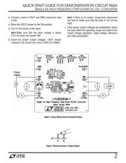
QUICK START PROCEDURE
Demonstration circuit 965A is easy to set up to evalu-
ate the performance of the LTC3835EGN-1. Refer to
Figure 1 for proper measurement equipment setup
and follow the procedure below:
NOTE:
When measuring the input or output voltage
ripple, care must be taken to avoid a long ground lead
on the oscilloscope probe. Measure the input or out-
put voltage ripple by touching the probe tip directly
across the Vin or Vout and GND terminals. See
Figure 2 for proper scope probe technique.
1.
Place VOUT jumper in the OFF position, the PLLPF
jumper (JP2) at the selected frequency and the
MODE jumper (JP3) in desired Mode (Burst, CCM
or DCM) position. Table 2 shows the default setting
for DC965A.
JP1
TRACK/SS
JP2 PLLPF JP3 MODE
JP4 V
OUT
SS 400kHz DCM ON
Table 2. Default Jumper Settings
2.
With power off, connect a 4.5V-36V, 6A power
supply to VIN and GND.