
herunterladen
QUICK START GUIDE FOR DEMONSTRATION CIRCUIT 616
4MHZ, POLYPHASE HIGH EFFICIENCY SYNCHRONOUS BOOST CONVERTER
1
LTC3425EUH
DESCRIPTION
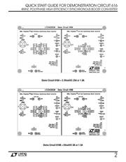
Demonstration Circuit 616 is a synchronous, 4-phase
boost converter using the LTC3425. It is capable of op-
erating below 1V input. DC616A is set for 3.3V output.
DC616B is set for 5V output. On each demo board, the
left circuit gives higher efficiency and current rating;
while the right circuit has smaller size and lower cost.
The switching frequency is set at 1MHz per phase,
minimizing inductor and capacitor size. A single resistor
at RT pin sets the frequency. If desired, the LTC3425
can be synchronized to an external clock.
Long wires run from input sources (such as wall adap-
tors) can cause large voltage spikes during initial plug-
in. C5 and C15 are installed on DC616 to damp the pos-
sible voltage spikes. They are not required for applica-
tions where input source is close to the regulator.
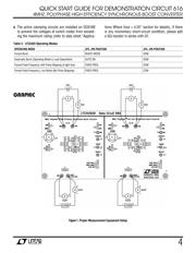
Please refer to Application Note 88 for details.
Design files for this circuit board are available. Call
the LTC factory.
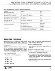
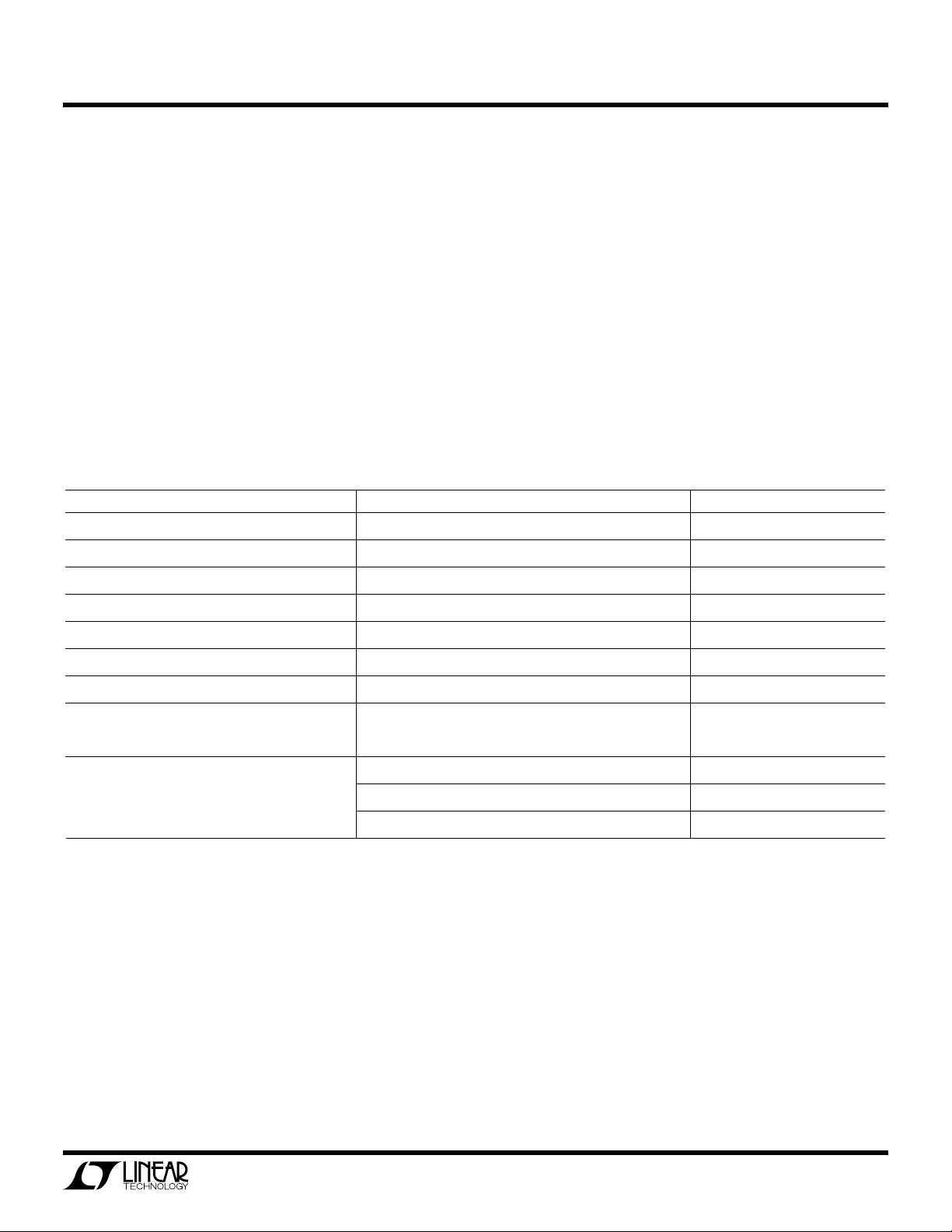
Table 1.
DC616A Performance Summary (T
A
= 25°C unless otherwise noted)
PARAMETER CONDITION VALUE
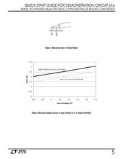
Minimum Input Voltage (Start-Up) 1V
Output Voltage V
OUT1
(High Efficiency Circuit) V
IN
= 2V to 3V, I
OUT1
= 0A to 2.25A 3.3V ±4%
Output Voltage V
OUT2
(Low Cost Circuit) V
IN
= 2V to 3V, I
OUT2
= 0A to 1.8A 3.3V ±4%
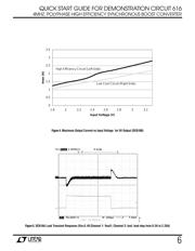
Maximum Output Current (High Efficiency Circuit) V
IN
= 2V to 3V 2.25A
Maximum Output Current (Low Cost Circuit) V
IN
= 2V to 3V 1.8A
Typical Output Ripple V
OUT
V
IN
= 2.4V, I
OUT
= 1.8A (20MHz BW) 28mV
P–P
Typical Switching Frequency (each phase) 1MHz
Efficiency (High Efficiency Circuit)
V
IN
= 2.4V, I
OUT1
= 0.5A
V
IN
= 2.4V, I
OUT1
= 2A
93.0% Typical
88.6% Typical
Logic Low Voltage-Off, -40
°
C to 85
°
C 0.25V MAX
Logic High Voltage-On (Initial Start-Up), -40
°
C to 85
°
C 1V MIN
On/Off Control
Logic High Voltage-On (V
OUT
>2.4V), -40
°
C to 85
°
C 0.65V MIN