
herunterladen
1
dc2414af
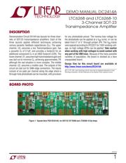
DEMO MANUAL DC2414A
Description
LTC6268 and LTC6268-10
3-Channel SOT-23
Transimpedance Amplifier
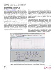
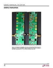
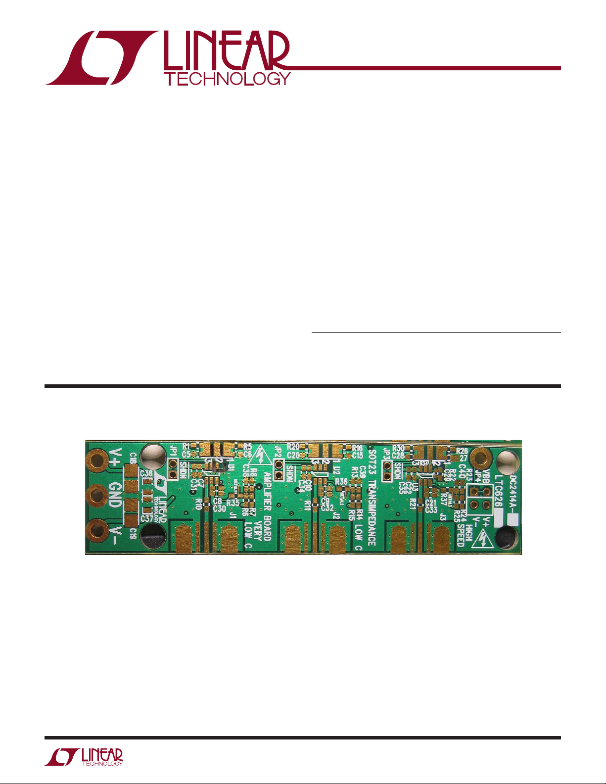
Demonstration Circuit 2414A has layouts for three chan-
nels of SOT-23 transimpedance amplifiers. Each of the
three layouts applies different techniques achieving
various parasitic feedback capacitances (C
F
). The upper
channel, U3, assumes a low Transimpedance gain, has
a parasitic C
F
of 0.1pF, and provides a footprint for an
additional component C
F
in an 0402 footprint (C29). The
lower channel, U1, assumes high transimpedance gain and
was laid out to minimize C
F
, achieving approximately 7fF,
although the real situation is more complex. The middle
channel, U2, assumes a middle case. The outputs of the
circuit are laid out for SMA edge connectors. The inputs
consist of six pads per channel along the edge where a
through-hole photodiode can be mounted, with provision
L, LT, LTC, LTM, Linear Technology and the Linear logo are registered trademarks of Linear
Technology Corporation. All other trademarks are the property of their respective owners.
BoarD photo
for any photodiode pinout. The reverse bias voltage for
the photodiode can be applied at a V
BB
turret, or can be
taken from V
+
or V
–
through jumper JP4. The V
BB
traces
were spaced according to IPC2221 for 150V working volt-
age, so high voltage APDs can be applied. Take caution
when working with high voltages to avoid contact with
any part of the VBB trace.
Because of the many possible
varieties of population, the board is stocked as a bare
unpopulated board.
Design files for this circuit board are available at
http://www.linear.com/demo/DC2414A
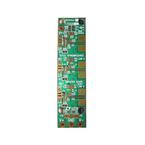
Figure 1. Topside Bare PCB DC2414A, for SOT-23 LTC
®
6268 and LTC6268-10 Op Amps